SNLS703 December   2023 DS90LVRA2-Q1

PRODUCTION DATA  

  1.   1
  2. Features
  3. Applications
  4. Description
  5. Pin Configuration and Functions
  6. Specifications
    1. 5.1 Absolute Maximum Ratings
    2. 5.2 ESD Ratings
    3. 5.3 Recommended Operating Conditions
    4. 5.4 Thermal Information
    5. 5.5 Electrical Characteristics
    6. 5.6 Switching Characteristics
    7. 5.7 Typical Characteristics
  7. Parameter Measurement Information
  8. Detailed Description
    1. 7.1 Overview
    2. 7.2 Functional Block Diagram
    3. 7.3 Feature Description
    4. 7.4 Device Functional Modes
  9. Application and Implementation
    1. 8.1 Application Information
    2. 8.2 Typical Application
      1. 8.2.1 Design Requirements
      2. 8.2.2 Detailed Design Procedure
        1. 8.2.2.1 Power Decoupling Recommendations
        2. 8.2.2.2 Termination
        3. 8.2.2.3 Input Failsafe Biasing
        4. 8.2.2.4 Probing LVDS Transmission Lines
      3. 8.2.3 Application Curves
    3. 8.3 Power Supply Recommendations
    4. 8.4 Layout
      1. 8.4.1 Layout Guidelines
        1. 8.4.1.1 Differential Traces
        2. 8.4.1.2 PC Board Considerations
      2. 8.4.2 Layout Examples
  10. Device and Documentation Support
    1. 9.1 Documentation Support
      1. 9.1.1 Related Documentation
    2. 9.2 Receiving Notification of Documentation Updates
    3. 9.3 Support Resources
    4. 9.4 Trademarks
    5. 9.5 Electrostatic Discharge Caution
    6. 9.6 Glossary
  11. 10Revision History
  12. 11Mechanical, Packaging, and Orderable Information

Package Options

Refer to the PDF data sheet for device specific package drawings

Mechanical Data (Package|Pins)
  • DEM|8
Thermal pad, mechanical data (Package|Pins)
Orderable Information

Description

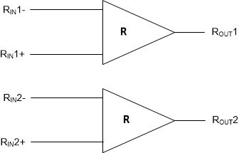
The DS90LVRA2-Q1 is a dual CMOS differential line receiver designed for applications requiring high input common mode range, high data rates, and CMOS output with slew rate control. The device is designed to support data rates of 600Mbps (300MHz) utilizing low voltage differential signaling (LVDS) technology.

The DS90LVRA2-Q1 accepts low voltage (350mV typical) differential input signals and translates them from 1.8V to 3.3V CMOS output levels depending on power supply voltage. The DS90LVRA2-Q1 has a flow-through design for easy PCB layout.

The DS90LVRA2-Q1 and companion LVDS line driver DS90LV027AQ provide a new alternative to high power PECL/ECL devices for high speed point-to-point interface applications.
Package Information
PART NUMBERPACKAGE(1)PACKAGE SIZE(2)
DS90LVRA2-Q1DEM (WSON, 8)2mm × 2mm
For more information, see Section 11.
The package size (length × width) is a nominal value and includes pins, where applicable.
GUID-4F112770-4856-448F-A197-479AA8C66C67-low.gifFunctional Diagram