SNLS703 December   2023 DS90LVRA2-Q1

PRODUCTION DATA  

  1.   1
  2. Features
  3. Applications
  4. Description
  5. Pin Configuration and Functions
  6. Specifications
    1. 5.1 Absolute Maximum Ratings
    2. 5.2 ESD Ratings
    3. 5.3 Recommended Operating Conditions
    4. 5.4 Thermal Information
    5. 5.5 Electrical Characteristics
    6. 5.6 Switching Characteristics
    7. 5.7 Typical Characteristics
  7. Parameter Measurement Information
  8. Detailed Description
    1. 7.1 Overview
    2. 7.2 Functional Block Diagram
    3. 7.3 Feature Description
    4. 7.4 Device Functional Modes
  9. Application and Implementation
    1. 8.1 Application Information
    2. 8.2 Typical Application
      1. 8.2.1 Design Requirements
      2. 8.2.2 Detailed Design Procedure
        1. 8.2.2.1 Power Decoupling Recommendations
        2. 8.2.2.2 Termination
        3. 8.2.2.3 Input Failsafe Biasing
        4. 8.2.2.4 Probing LVDS Transmission Lines
      3. 8.2.3 Application Curves
    3. 8.3 Power Supply Recommendations
    4. 8.4 Layout
      1. 8.4.1 Layout Guidelines
        1. 8.4.1.1 Differential Traces
        2. 8.4.1.2 PC Board Considerations
      2. 8.4.2 Layout Examples
  10. Device and Documentation Support
    1. 9.1 Documentation Support
      1. 9.1.1 Related Documentation
    2. 9.2 Receiving Notification of Documentation Updates
    3. 9.3 Support Resources
    4. 9.4 Trademarks
    5. 9.5 Electrostatic Discharge Caution
    6. 9.6 Glossary
  11. 10Revision History
  12. 11Mechanical, Packaging, and Orderable Information

Package Options

Refer to the PDF data sheet for device specific package drawings

Mechanical Data (Package|Pins)
  • DEM|8
Thermal pad, mechanical data (Package|Pins)
Orderable Information

Pin Configuration and Functions

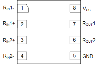
GUID-A4987E13-175B-47E7-BBC1-84A79FB7A9F7-low.gifFigure 4-1 DEM Package, WSON 8 Pin (Top View)
Table 4-1 Pin Functions
PIN TYPE(1) DESCRIPTION
NAME NO.
GND 5 G Ground pin
RIN1- 1 I Inverting receiver input pin
RIN2- 4 I
RIN1+ 2 I Non-inverting receiver input pin
RIN2+ 3 I
ROUT2 6 O Receiver output pin
ROUT1 7 O
VCC 8 P Power supply pin
I = input, O = output, G = ground