SNLS564B December 2017 – January 2024 FPC202
PRODUCTION DATA
- 1
- 1 Features
- 2 Applications
- 3 Description
- 4 Device Comparison Table
- 5 Pin Configuration and Functions
- 6 Specifications
-
7 Detailed Description
- 7.1 Overview
- 7.2 Functional Block Diagram
- 7.3
Feature Description
- 7.3.1 Host-Side Control Interface
- 7.3.2 LED Control
- 7.3.3 Low-Speed Output Signal Control
- 7.3.4 Low-Speed Input Status and Interrupt Generation
- 7.3.5 Downstream (Port-Side) I2C Master
- 7.3.6 Data Pre-Fetch From Modules
- 7.3.7 Scheduled Write
- 7.3.8 Protocol Timeouts
- 7.3.9 General-Purpose Inputs/Outputs
- 7.3.10 Hot-Plug Support
- 7.4 Device Functional Modes
- 7.5 Programming
- 8 Application and Implementation
- 9 Device and Documentation Support
- 10Revision History
- 11Mechanical, Packaging, and Orderable Information
Package Options
Refer to the PDF data sheet for device specific package drawings
Mechanical Data (Package|Pins)
- RHU|56
Thermal pad, mechanical data (Package|Pins)
Orderable Information
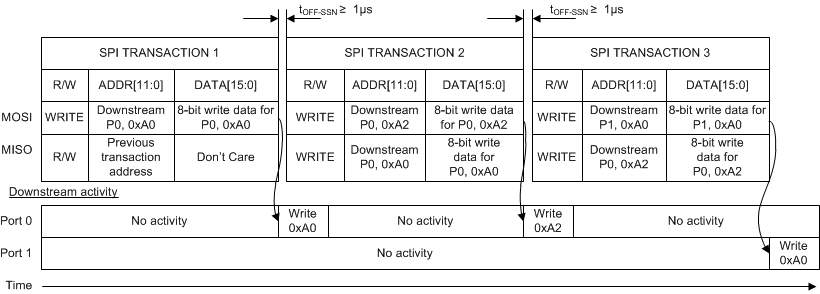
7.4.2.3 SPI Write Operation
Writing data to an FPC202 device or the downstream ports under its management requires one SPI transactions. Multiple write transactions to downstream ports can proceed with minimal delay provided that different ports are being written to. If attempting to write data to the same downstream port, then the corresponding downstream access delay, tOFF-SSN, is required. Figure 7-12 shows an example of writing to both downstream ports in succession.
 Figure 7-12 SPI Writes To Both Downstream Ports In Succession