SBOS027C September 2000 – September 2022 INA118
PRODUCTION DATA
- 1 Features
- 2 Applications
- 3 Description
- 4 Revision History
- 5 Device Comparison Table
- 6 Pin Configuration and Functions
- 7 Specifications
- 8 Detailed Description
- 9 Application and Implementation
- 10Device and Documentation Support
- 11Mechanical, Packaging, and Orderable Information
Package Options
Mechanical Data (Package|Pins)
Thermal pad, mechanical data (Package|Pins)
Orderable Information
9.3.1 Low-Voltage Operation
The INA118 operates on power supplies as low as ±2.25 V. Performance of the INA118 remains excellent with power supplies ranging from ±2.25 V to ±18 V. Most parameters vary only slightly throughout this supply voltage range; see also Section 7.6. Operation at low supply voltage requires careful attention to make sure that the input voltages remain within the respective linear range. Voltage swing requirements of internal nodes limit the input common-mode range with low power supply voltage. Figure 7-3 shows the range of linear operation for a various supply voltages and gains.
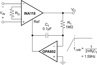
 Figure 9-6 AC-Coupled Instrumentation Amplifier
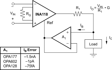
 Figure 9-8 Differential Voltage to Current Converter
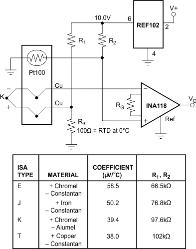
 Figure 9-7 Thermocouple Amplifier With Cold Junction Compensation
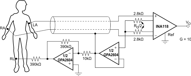
 Figure 9-9 ECG Amplifier With Right-Leg Drive