-
INA20x High-Side Measurement Current-Shunt Monitor With Open-Drain Comparator and Reference
- 1 Features
- 2 Applications
- 3 Description
- 4 Revision History
- 5 Pin Configuration and Functions
- 6 Specifications
- 7 Detailed Description
- 8 Application and Implementation
- 9 Power Supply Recommendations
- 10Layout
- 11Device and Documentation Support
- 12Mechanical, Packaging, and Orderable Information
- IMPORTANT NOTICE
Package Options
Mechanical Data (Package|Pins)
Thermal pad, mechanical data (Package|Pins)
Orderable Information
INA20x High-Side Measurement Current-Shunt Monitor With Open-Drain Comparator and Reference
1 Features
- Complete Current Sense Solution
- Three Gain Options Available:
- INA200 = 20 V/V
- INA201 = 50 V/V
- INA202 = 100 V/V
- 0.6-V Internal Voltage Reference
- Internal Open-Drain Comparator
- Latching Capability on Comparator
- Common-Mode Range: –16 V to 80 V
- High Accuracy: 3.5% Maximum Error Over Temperature
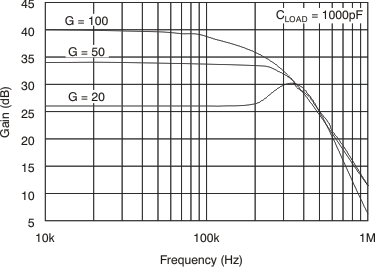
- Bandwidth: 500 kHz (INA200)
- Quiescent Current: 1800 μA (Maximum)
- Packages: SOIC-8, VSSOP-8
2 Applications
- Notebook Computers
- Cell Phones
- Telecom Equipment
- Automotive
- Power Management
- Battery Chargers
- Welding Equipment
3 Description
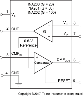
The INA200, INA201, and INA202 devices are high-side current-shunt monitors with voltage output and integrated comparator. The INA20x devices can sense drops across shunts at common-mode voltages from –16 V to 80 V. The INA20x series is available with three output voltage scales: 20 V/V, 50 V/V, and 100 V/V, with a bandwidth up to 500-kHz.
The INA200, INA201, and INA202 devices incorporate an open-drain comparator and internal reference providing a 0.6-V threshold. External dividers set the current trip point. The comparator includes a latching capability, that can be made transparent by grounding (or leaving open) the RESET pin.
The INA200, INA201, and INA202 devices operate from a single 2.7-V to 18-V supply, drawing a maximum of 1800 μA of supply current. Package options include the very small VSSOP-8 and the
SOIC-8. All versions are specified over the extended operating temperature range of –40°C to +125°C.
Device Information(1)
| PART NUMBER | PACKAGE | BODY SIZE (NOM) |
|---|---|---|
| INA200 INA201 INA202 |
SOIC (8) | 4.90 mm × 3.91 mm |
| VSSOP (8) | 3.00 mm × 3.00 mm |
- For all available packages, see the orderable addendum at the end of the data sheet.
Simplified Schematic
4 Revision History
Changes from D Revision (October 2015) to E Revision
- Reformatted Thermal Information table note Go
- Corrected typo in Voltage Output section in Electrical Characteristics tableGo
- Added text to Comparator subsection in Feature Description sectionGo
- Added Figure 31 to Feature Description sectionGo
- Added Output vs Supply Ramp Considerations subsection in Feature Description sectionGo
- Added Figure 36, Figure 37, and Figure 38Go
Changes from C Revision (October 2010) to D Revision
- Added ESD Ratings table, Thermal Information table, Feature Description section, Device Functional Modes, Application and Implementation section, Power Supply Recommendations section, Layout section, Device and Documentation Support section, and Mechanical, Packaging, and Orderable Information section Go
Changes from B Revision (October, 2007) to C Revision
5 Pin Configuration and Functions
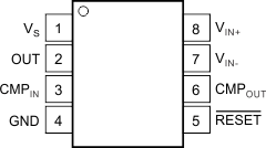
Pin Functions
| PIN | I/O | DESCRIPTION | |
|---|---|---|---|
| NAME | NO. | ||
| CMPIN | 3 | Analog input | Comparator input |
| CMPOUT | 6 | Analog output | Comparator output |
| GND | 4 | Analog | Ground |
| OUT | 2 | Analog output | Output voltage |
| RESET | 5 | Analog input | Comparator reset pin, active low |
| VIN– | 7 | Analog input | Connect to shunt low side |
| VIN+ | 8 | Analog input | Connect to shunt high side |
| VS | 1 | Analog | Power supply |
6 Specifications
6.1 Absolute Maximum Ratings
over operating free-air temperature range (unless otherwise noted)(1)| MIN | MAX | UNIT | ||
|---|---|---|---|---|
| Supply voltage, Vs | 2.7 | 18 | V | |
| Current-shunt monitor analog inputs, VIN+, VIN– | Differential (VIN+) – (VIN–) | –18 | 18 | V |
| Common-mode(2) | –16 | 80 | V | |
| Comparator analog input and reset pins(2) | GND – 0.3 | (Vs) + 0.3 | V | |
| Analog output, OUT(2) | GND – 0.3 | (Vs) + 0.3 | V | |
| Comparator output, OUT(2) | GND – 0.3 | 18 | V | |
| Input current into any pin(2) | 5 | mA | ||
| Operating temperature | –55 | 150 | °C | |
| Junction temperature | –65 | 150 | °C | |
| Storage temperature, Tstg | –65 | 150 | °C | |
6.2 ESD Ratings
| VALUE | UNIT | ||||
|---|---|---|---|---|---|
| V(ESD) | Electrostatic discharge | Human body model (HBM), per ANSI/ESDA/JEDEC JS-001, all pins(1) | ±4000 | V | |
| Charged device model (CDM), per JEDEC specification JESD22-C101, all pins(2) | ±1000 | ||||
6.3 Recommended Operating Conditions
over operating free-air temperature range (unless otherwise noted)| MIN | NOM | MAX | UNIT | ||
|---|---|---|---|---|---|
| VCM | Common-mode input voltage | –16 | 12 | 80 | V |
| VS | Operating supply voltage | 2.7 | 12 | 18 | V |
| TA | Operating free-air temperature | –40 | 25 | 125 | °C |
6.4 Thermal Information
| THERMAL METRIC(1) | INA20x | UNIT | ||
|---|---|---|---|---|
| D (SOIC) | DGK (SOIC) | |||
| 8 PINS | 8 PINS | |||
| RθJA | Junction-to-ambient thermal resistance | 110.5 | 162.2 | °C/W |
| RθJC(top) | Junction-to-case (top) thermal resistance | 50.4 | 37.7 | °C/W |
| RθJB | Junction-to-board thermal resistance | 52.7 | 82.9 | °C/W |
| ψJT | Junction-to-top characterization parameter | 7.8 | 1.3 | °C/W |
| ψJB | Junction-to-board characterization parameter | 51.9 | 81.4 | °C/W |
6.5 Electrical Characteristics: Current-Shunt Monitor
at TA = 25°C, VS = 12 V, VCM = 12 V, VSENSE = 100 mV, RL = 10 kΩ to GND, RPULL-UP = 5.1 kΩ connected from CMPOUT to VS, and CMPIN = GND, (unless otherwise noted)| PARAMETER | TEST CONDITIONS | MIN | TYP | MAX | UNIT | |||
|---|---|---|---|---|---|---|---|---|
| INPUT | ||||||||
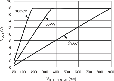
| VSENSE | Full-scale sense input voltage | VSENSE = VIN+ – VIN– | 0.15 | (VS – 0.25) / Gain | V | |||
| VCM | Common-mode input range | TA = –40°C to 125°C | –16 | 80 | V | |||
| CMR | Common-mode rejection | VIN+ = –16 V to 80 V | 80 | 100 | dB | |||
| VIN+ = 12 V to 80 V, TA = –40°C to 125°C | 100 | 123 | dB | |||||
| VOS | Offset voltage, RTI(1) | TA = 25°C | ±0.5 | ±2.5 | mV | |||
| TA = 25°C to 125°C | ±3 | mV | ||||||
| TA = –40°C to 25°C | ±3.5 | mV | ||||||
| dVOS/dT | Offset voltage, RTI, vs temperature | TMIN to TMAX, TA = –40°C to 125°C | 5 | μV/°C | ||||
| PSR | Offset voltage, RTI, vs power supply | VOUT = 2 V, VIN+ = 18 V, 2.7 V, TA = –40°C to 125°C | 2.5 | 100 | μV/V | |||
| IB | Input bias current, VIN– pin | TA = –40°C to 125°C | ±9 | ±16 | μA | |||
| OUTPUT (VSENSE ≥ 20 mV) | ||||||||
| G | Gain | INA200 | 20 | V/V | ||||
| INA201 | 50 | V/V | ||||||
| INA202 | 100 | V/V | ||||||
| Gain error | VSENSE = 20 mV to 100 mV | ±0.2% | ±1% | |||||
| VSENSE = 20 mV to 100 mV, TA = –40°C to 125°C | ±2% | |||||||
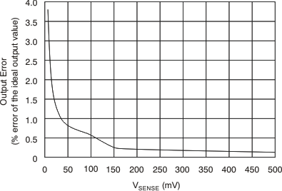
| Total output error(2) | VSENSE = 120 mV, VS = 16 V | ±0.75% | ±2.2% | |||||
| VSENSE = 120 mV, VS = 16 V, TA = –40°C to 125°C | ±3.5% | |||||||
| Nonlinearity error(3) | VSENSE = 20 mV to 100 mV | ±0.002% | ||||||
| RO | Output impedance | 1.5 | Ω | |||||
| Maximum capacitive load | No sustained oscillation | 10 | nF | |||||
| OUTPUT (VSENSE < 20 mV)(4) | ||||||||
| Output | INA200, INA201, INA202 | –16 V ≤ VCM < 0 V | 300 | mV | ||||
| INA200 | 0 V ≤ VCM ≤ VS, VS = 5 V | 0.4 | V | |||||
| INA201 | 0 V ≤ VCM ≤ VS, VS = 5 V | 1 | V | |||||
| INA202 | 0 V ≤ VCM ≤ VS, VS = 5 V | 2 | V | |||||
| INA200, INA201, INA202 | VS < VCM ≤ 80 V | 300 | mV | |||||
| VOLTAGE OUTPUT(5) | ||||||||
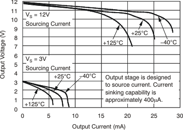
| Output swing to the positive rail | VIN– = 11 V, VIN+ = 12 V, TA = –40°C to 125°C | (Vs) – 0.15 | (Vs) – 0.25 | V | ||||
| Output swing to GND(6) | VIN– = 0 V, VIN+ = –0.5 V, TA = –40°C to 125°C | (GND) + 0.004 | (GND) + 0.05 | V | ||||
| FREQUENCY RESPONSE | ||||||||
| BW | Bandwidth | INA200 | CLOAD = 5 pF | 500 | kHz | |||
| INA201 | CLOAD = 5 pF | 300 | kHz | |||||
| INA202 | CLOAD = 5 pF | 200 | kHz | |||||
| Phase margin | CLOAD < 10 nF | 40 | °C | |||||
| SR | Slew rate | 1 | V/μs | |||||
| Settling time (1%) | VSENSE = 10 mVPP to 100 mVPP, CLOAD = 5 pF |
2 | μs | |||||
| NOISE, RTI | ||||||||
| Voltage noise density | 40 | nV/√Hz | ||||||
6.6 Electrical Characteristics: Comparator
at TA = 25°C, VS = 12 V, VCM = 12 V, VSENSE = 100 mV, RL = 10 kΩ to GND, and RPULL-UP = 5.1 kΩ connected from CMPOUT to VS, (unless otherwise noted)| PARAMETER | TEST CONDITIONS | MIN | TYP | MAX | UNIT | ||
|---|---|---|---|---|---|---|---|
| OFFSET VOLTAGE | |||||||
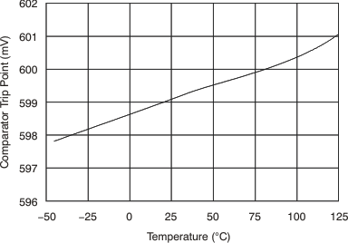
| Threshold | TA = 25°C | 590 | 608 | 620 | mV | ||
| TA = –40°C to 125°C | 586 | 625 | mV | ||||
| Hysteresis(1) | TA = –40°C to 85°C | –8 | mV | ||||
| INPUT BIAS CURRENT(2) | |||||||
| Input bias current, CMPin PIN | 0.005 | 10 | nA | ||||
| Input bias current, CMPin PIN, vs temperature | TA = –40°C to 125°C | 15 | nA | ||||
| INPUT VOLTAGE RANGE | |||||||
| Input voltage range, CMPin PIN | 0 V to VS – 1.5 V | V | |||||
| OUTPUT (OPEN-DRAIN) | |||||||
| Large-signal differential voltage gain | CMP VOUT 1 V to 4 V, RL ≥ 15 kΩ connected to 5 V |
200 | V/mV | ||||
| ILKG | High-level leakage current(3)(4) | VID = 0.4 V, VOH = VS | 0.0001 | 1 | μA | ||
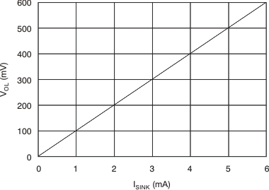
| VOL | Low-level output voltage(3) | VID = –0.6 V, IOL = 2.35 mA | 220 | 300 | mV | ||
| RESPONSE TIME | |||||||
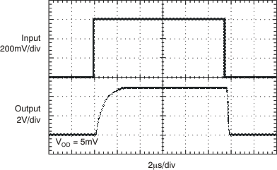
| Response time(5) | RL to 5 V, CL = 15 pF, 100-mV Input Step with 5-mV overdrive | 1.3 | μs | ||||
| RESET | |||||||
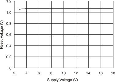
| RESET threshold(6) | 1.1 | V | |||||
| Logic input impedance | 2 | MΩ | |||||
| Minimum RESET pulse width | 1.5 | μs | |||||
| RESET propagation delay | 3 | μs | |||||
6.7 Electrical Characteristics: General
at TA = 25°C, VS = 12 V, VCM = 12 V, VSENSE = 100 mV, RL = 10 kΩ to GND, RPULL-UP = 5.1 kΩ connected from CMPOUT to VS, and CMPIN = 1 V, unless otherwise noted.| PARAMETER | TEST CONDITIONS | MIN | TYP | MAX | UNIT | ||
|---|---|---|---|---|---|---|---|
| POWER SUPPLY | |||||||
| VS | Operating power supply | TA = –40°C to 125°C | 2.7 | 18 | V | ||
| IQ | Quiescent current | VOUT = 2 V | 1350 | 1800 | μA | ||
| VSENSE = 0 mV, TA = –40°C to 125°C | 1850 | μA | |||||
| Comparator power-on reset threshold(1) | 1.5 | V | |||||
| TEMPERATURE | |||||||
| Specified temperature | –40 | 125 | °C | ||||
| Operating temperature | –55 | 150 | °C | ||||
| Storage temperature | –65 | 150 | °C | ||||
| θJA | Thermal resistance | VSSOP-8 Surface-Mount | 200 | °C/W | |||
| SOIC-8 | 150 | °C/W | |||||
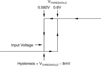 Figure 1. Typical Comparator Hysteresis
6.8 Typical Characteristics
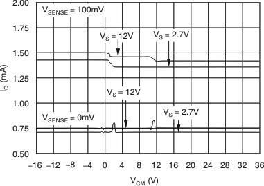
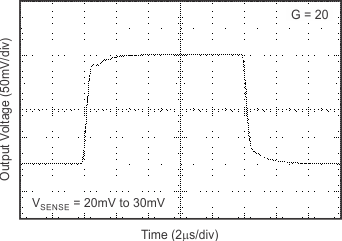
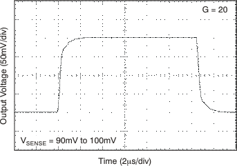
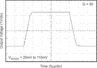
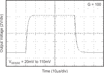
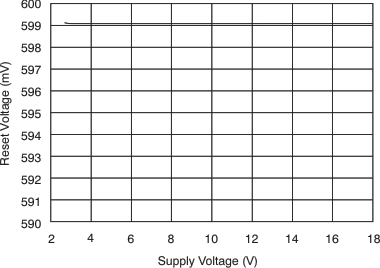
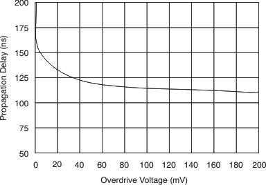
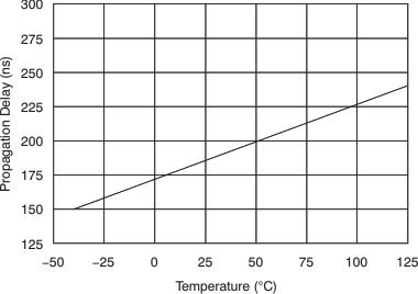
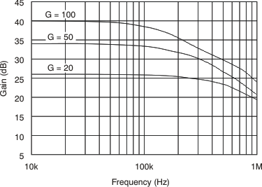
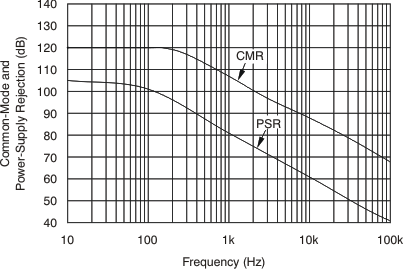
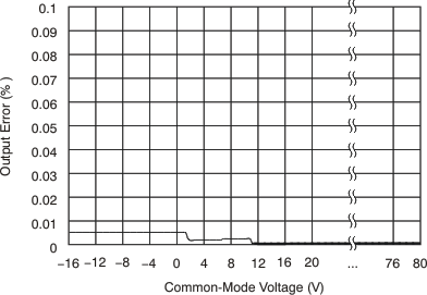
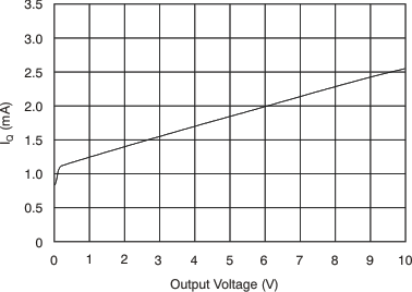
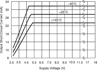
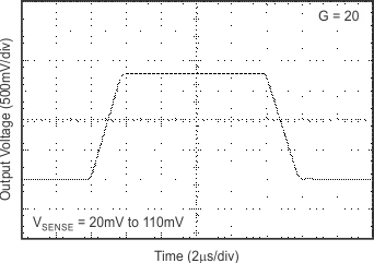
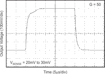
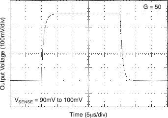
at TA = 25°C, VS = 12 V, VIN+ = 12 V, and VSENSE = 100 mV, (unless otherwise noted)