SBOS374E November   2006  – September 2017 INA200 , INA201 , INA202

PRODUCTION DATA.  

  1. Features
  2. Applications
  3. Description
  4. Revision History
  5. Pin Configuration and Functions
  6. Specifications
    1. 6.1 Absolute Maximum Ratings
    2. 6.2 ESD Ratings
    3. 6.3 Recommended Operating Conditions
    4. 6.4 Thermal Information
    5. 6.5 Electrical Characteristics: Current-Shunt Monitor
    6. 6.6 Electrical Characteristics: Comparator
    7. 6.7 Electrical Characteristics: General
    8. 6.8 Typical Characteristics
  7. Detailed Description
    1. 7.1 Overview
    2. 7.2 Functional Block Diagram
    3. 7.3 Feature Description
      1. 7.3.1 Basic Connections
      2. 7.3.2 Selecting RS
      3. 7.3.3 Comparator
    4. 7.4 Device Functional Modes
      1. 7.4.1 Input Filtering
      2. 7.4.2 Accuracy Variations as a Result of VSENSE and Common-Mode Voltage
        1. 7.4.2.1 Normal Case 1: VSENSE ≥ 20 mv, VCM ≥ VS
        2. 7.4.2.2 Normal Case 2: VSENSE ≥ 20 mv, VCM < VS
        3. 7.4.2.3 Low VSENSE Case 1: VSENSE < 20 mV, -16 V ≤ VCM < 0 and Low VSENSE Case 3: VSENSE < 20 mV, VS < VCM ≤ 80 V
        4. 7.4.2.4 Low VSENSE Case 2: VSENSE < 20 mV, 0 V ≤ VCM ≤ VS
      3. 7.4.3 Transient Protection
      4. 7.4.4 Output Voltage Range
  8. Application and Implementation
    1. 8.1 Application Information
    2. 8.2 Typical Application
      1. 8.2.1 Design Requirements
      2. 8.2.2 Detailed Design Procedure
      3. 8.2.3 Application Curve
  9. Power Supply Recommendations
    1. 9.1 Output vs Supply Ramp Considerations
  10. 10Layout
    1. 10.1 Layout Guidelines
    2. 10.2 Layout Example
  11. 11Device and Documentation Support
    1. 11.1 Related Links
    2. 11.2 Community Resources
    3. 11.3 Trademarks
    4. 11.4 Electrostatic Discharge Caution
    5. 11.5 Glossary
  12. 12Mechanical, Packaging, and Orderable Information

Package Options

Mechanical Data (Package|Pins)
Thermal pad, mechanical data (Package|Pins)
Orderable Information

Pin Configuration and Functions

DGK and D Packages
8-Pin VSSOP and SOIC
Top View
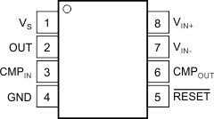
INA200 INA201 INA202 po_bos374.gif

Pin Functions

PIN I/O DESCRIPTION
NAME NO.
CMPIN 3 Analog input Comparator input
CMPOUT 6 Analog output Comparator output
GND 4 Analog Ground
OUT 2 Analog output Output voltage
RESET 5 Analog input Comparator reset pin, active low
VIN– 7 Analog input Connect to shunt low side
VIN+ 8 Analog input Connect to shunt high side
VS 1 Analog Power supply