SBOS539A December 2010 – April 2016 INA203-Q1
PRODUCTION DATA.
- 1 Features
- 2 Applications
- 3 Description
- 4 Revision History
- 5 Device Comparison Table
- 6 Pin Configuration and Functions
-
7 Specifications
- 7.1 Absolute Maximum Ratings
- 7.2 ESD Ratings
- 7.3 Recommended Operating Conditions
- 7.4 Thermal Information
- 7.5 Electrical Characteristics: Current-Shunt Monitor
- 7.6 Electrical Characteristics: Comparator
- 7.7 Electrical Characteristics: Reference
- 7.8 Electrical Characteristics: General
- 7.9 Typical Characteristics
- 8 Detailed Description
- 9 Application and Implementation
- 10Power Supply Recommendations
- 11Layout
- 12Device and Documentation Support
- 13Mechanical, Packaging, and Orderable Information
Package Options
Mechanical Data (Package|Pins)
- PW|14
Thermal pad, mechanical data (Package|Pins)
Orderable Information
7 Specifications
7.1 Absolute Maximum Ratings
over operating free-air temperature range (unless otherwise noted) (1)(1) Stresses beyond those listed under Absolute Maximum Ratings may cause permanent damage to the device. These are stress ratings only, which do not imply functional operation of the device at these or any other conditions beyond those indicated under Recommended Operating Conditions. Exposure to absolute-maximum-rated conditions for extended periods may affect device reliability.
7.2 ESD Ratings
| VALUE | UNIT | |||
|---|---|---|---|---|
| V(ESD) | Electrostatic discharge | Human-body model (HBM), per AEC Q100-002(1) | ±2000 | V |
| Charged-device model (CDM), per AEC Q100-011 | ±500 | |||
(1) AEC Q100-002 indicates that HBM stressing shall be in accordance with the ANSI/ESDA/JEDEC JS-001 specification.
7.3 Recommended Operating Conditions
over operating free-air temperature range (unless otherwise noted)| MIN | NOM | MAX | UNIT | ||
|---|---|---|---|---|---|
| VCM | Common-mode input voltage | –16 | 12 | 80 | V |
| VS | Operating supply voltage | 2.7 | 12 | 18 | V |
| TA | Operating free-air temperature | –40 | 25 | 125 | ºC |
7.4 Thermal Information
| THERMAL METRIC(1) | INA203-Q1 | UNIT | |
|---|---|---|---|
| PW (TSSOP) | |||
| 14 PINS | |||
| RθJA | Junction-to-ambient thermal resistance | 112.6 | °C/W |
| RθJC(top) | Junction-to-case (top) thermal resistance | 37.2 | °C/W |
| RθJB | Junction-to-board thermal resistance | 55.4 | °C/W |
| ψJT | Junction-to-top characterization parameter | 2.7 | °C/W |
| ψJB | Junction-to-board characterization parameter | 54.7 | °C/W |
| RθJC(bot) | Junction-to-case (bottom) thermal resistance | 150 | °C/W |
(1) For more information about traditional and new thermal metrics, see the Semiconductor and IC Package Thermal Metrics application report, SPRA953.
7.5 Electrical Characteristics: Current-Shunt Monitor
At TA = 25°C, VS = 12 V, VCM = 12 V, VSENSE = 100 mV, RL = 10 kΩ to GND, RPULL-UP = 5.1 kΩ each connected from CMP1 OUT and CMP2 OUT to VS, and CMP1 IN+ = 1 V and CMP2 IN+ = GND, unless otherwise noted.| PARAMETER | TEST CONDITIONS | MIN | TYP | MAX | UNIT | |||||
|---|---|---|---|---|---|---|---|---|---|---|
| INPUT | ||||||||||
| VSENSE | Full-scale sense input voltage | VSENSE = VIN+ – VIN– | 0.15 | (VS – 0.25)/Gain | V | |||||
| VCM | Common-mode input range | TA = –40°C to +125°C | –16 | 80 | V | |||||
| CMRR | Common-mode rejection ratio | VCM = –16 V to +80 V | 80 | 100 | dB | |||||
| Over temperature | VCM = 12 V to 80 V | TA = 25°C to 125°C | 100 | 123 | dB | |||||
| TA = –40°C to +25°C | 90 | 100 | dB | |||||||
| VOS | Offset voltage, RTI(1) | ±0.5 | ±2.5 | mV | ||||||
| TA = 25°C to 125°C | ±3 | mV | ||||||||
| TA = –40°C to +25°C | ±3.5 | mV | ||||||||
| dVOS/dT | Versus temperature | TMIN to TMAX | TA = –40°C to +125°C | 5 | μV/°C | |||||
| PSR | Versus power supply | VOUT = 2 V, VCM = +18 V | TA = –40°C to +125°C | 2.5 | 100 | μV/V | ||||
| IB | Input bias current, VIN– Pin | TA = –40°C to +125°C | ±9 | ±16 | μA | |||||
| OUTPUT (VSENSE ≥ 20 mV) | ||||||||||
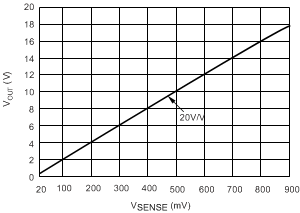
| G | Gain | 20 | V/V | |||||||
| Gain error | VSENSE = 20 mV to 100 mV | ±0.2% | ±1% | |||||||
| Over temperature | VSENSE = 20 mV to 100 mV | TA = –40°C to +125°C | ±2% | |||||||
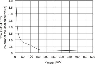
| Total output error(2) | VSENSE = 120 mV, VS = +16 V | ±0.75% | ±2.2% | |||||||
| Over temperature | VSENSE = 120 mV, VS = +16 V | TA = –40°C to +125°C | ±3.5% | |||||||
| Nonlinearity error(3) | VSENSE = 20 mV to 100 mV | ±0.002% | ||||||||
| RO | Output impedance, Pin 2 | 1.5 | Ω | |||||||
| Maximum capacitive load | No sustained oscillation | 10 | nF | |||||||
| OUTPUT (VSENSE < 20 mV)(4) | ||||||||||
| VOUT | Output voltage | –16 V ≤ VCM < 0 V | 300 | mV | ||||||
| 0 V ≤ VCM ≤ VS, VS = 5 V | 0.4 | V | ||||||||
| VS < VCM ≤ 80 V | 300 | mV | ||||||||
| VOLTAGE OUTPUT(5) | ||||||||||
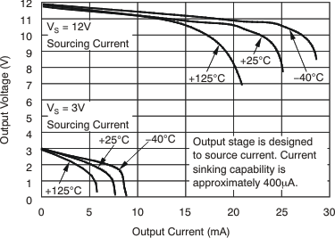
| Output swing to the positive rail | VIN– = 11 V, VIN+ = 12 V | TA = –40°C to +125°C | (VS) – 0.15 | (VS) – 0.25 | V | |||||
| Output Swing to GND(6) | VIN– = 0 V, VIN+ = –0.5 V | TA = –40°C to +125°C | (VGND) + 0.004 | (VGND) + 0.05 | V | |||||
| FREQUENCY RESPONSE | ||||||||||
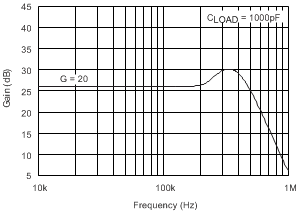
| BW | Bandwidth | CLOAD = 5 pF | 500 | kHz | ||||||
| Phase margin | CLOAD < 10 nF | 40 | Degrees | |||||||
| SR | Slew rate | 1 | V/μs | |||||||
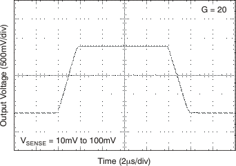
| Settling time (1%) | VSENSE = 10 mVPP to 100 mVPP, CLOAD = 5 pF |
2 | μs | |||||||
| NOISE, RTI | ||||||||||
| Output Voltage Noise Density | 40 | nV/√Hz | ||||||||
(1) Offset is extrapolated from measurements of the output at 20 mV and 100 mV VSENSE.
(2) Total output error includes effects of gain error and VOS.
(3) Linearity is best fit to a straight line.
(4) For details on this region of operation, see the Accuracy Variations section.
(5) See Typical Characteristics curve Positive Output Voltage Swing vs Output Current (Figure 8).
(6) Specified by design; not production tested.
7.6 Electrical Characteristics: Comparator
At TA = +25°C, VS = +12 V, VCM = +12 V, VSENSE = 100 mV, RL = 10 kΩ to GND, and RPULL-UP = 5.1 kΩ each connected from CMP1 OUT and CMP2 OUT to VS, unless otherwise noted.| PARAMETER | TEST CONDITIONS | MIN | TYP | MAX | UNIT | ||
|---|---|---|---|---|---|---|---|
| OFFSET VOLTAGE | |||||||
| Offset voltage | Comparator common-mode voltage = threshold voltage | 2 | mV | ||||
| Offset voltage drift, comparator 1 | TA = –40°C to +125°C | ±2 | μV/°C | ||||
| Offset voltage drift, comparator 2 | TA = –40°C to +125°C | 5.4 | μV/°C | ||||
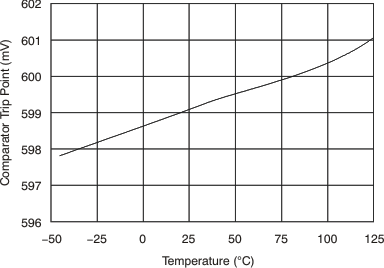
| Threshold | Rising Edge on Non-Inverting input, TA = +25°C | 590 | 608 | 620 | mV | ||
| Over temperature | TA = –40°C to +125°C | 586 | 625 | mV | |||
| Hysteresis(1), CMP1 | TA = –40°C to +85°C | –8 | mV | ||||
| Hysteresis(1), CMP2 | TA = –40°C to +85°C | 8 | mV | ||||
| INPUT BIAS CURRENT(2) | |||||||
| CMP1 IN+, CMP2 IN+ | 0.005 | 10 | nA | ||||
| Over temperature | TA = –40°C to +125°C | 15 | nA | ||||
| INPUT IMPEDANCE | |||||||
| Pins 3 and 6 | 10 | kΩ | |||||
| INPUT RANGE | |||||||
| CMP1 IN+ and CMP2 IN+ | 0 V to VS – 1.5 V | V | |||||
| Pins 3 and 6(3) | 0 V to VS – 1.5 V | V | |||||
| OUTPUT | |||||||
| Large-signal differential voltage gain | CMP VOUT 1 V to 4 V, RL ≥ 15 kΩ connected to 5 V | 200 | V/mV | ||||
| High-level output current | VID = 0.4 V, VOH = VS | 0.0001 | 1 | μA | |||
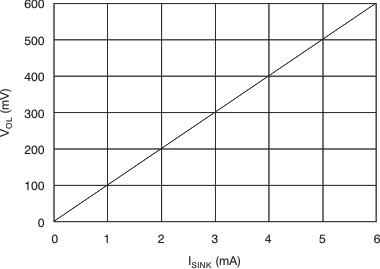
| Low-level output voltage | VID = –0.6 V, IOL = 2.35 mA | 220 | 300 | mV | |||
| RESPONSE TIME(4) | |||||||
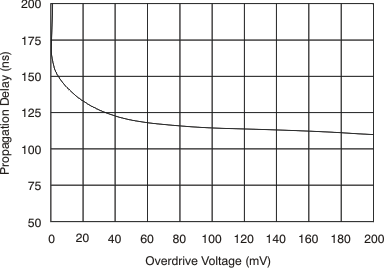
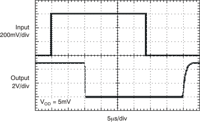
| Comparator 1 | RL to 5 V, CL = 15 pF, 100 mV input step with 5 mV overdrive | 1.3 | μs | ||||
| Comparator 2 | RL to 5 V, CL = 15 pF, 100 mV input step with 5 mV overdrive, CDELAY pin open | 1.3 | μs | ||||
| RESET | |||||||
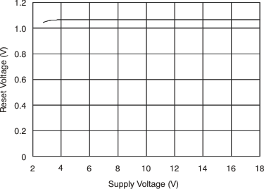
| RESET threshold(5) | 1.1 | V | |||||
| Logic input impedance | 2 | MΩ | |||||
| Minimum RESET pulse width | 1.5 | μs | |||||
| RESET propagation delay | 3 | μs | |||||
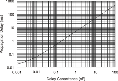
| Comparator 2 delay equation(6) | CDELAY = tD/5 | μF | |||||
| tD | Comparator 2 delay | CDELAY = 0.1 μF | 0.5 | s | |||
(1) Hysteresis refers to the threshold (the threshold specification applies to a rising edge of a noninverting input) of a falling edge on the noninverting input of the comparator; refer to Figure 1.
(2) Specified by design; not production tested.
(3) See the Comparator Maximum Input Voltage Range section.
(4) The comparator response time specified is the interval between the input step function and the instant when the output crosses 1.4 V.
(5) The CMP1 RESET input has an internal 2 MΩ (typical) pull-down. Leaving the CMP1 RESET open results in a LOW state, with transparent comparator operation.
(6) The Comparator 2 delay applies to both rising and falling edges of the comparator output.
7.7 Electrical Characteristics: Reference
At TA = +25°C, VS = +12 V, VCM = +12 V, VSENSE = 100 mV, RL = 10 kΩ to GND, and RPULL-UP = 5.1 kΩ each connected from CMP1 OUT and CMP2 OUT to VS, unless otherwise noted.| PARAMETER | TEST CONDITIONS | MIN | TYP | MAX | UNIT | |||||||
|---|---|---|---|---|---|---|---|---|---|---|---|---|
| REFERENCE VOLTAGE | ||||||||||||
| 1.2 VREFOUT output voltage | 1.188 | 1.2 | 1.212 | V | ||||||||
| dVOUT/dT | Reference drift(1) | TA = –40°C to +85°C | 40 | 100 | ppm/°C | |||||||
| 0.6 VREF | Output voltage (Pins 3 and 6) | 0.6 | V | |||||||||
| dVOUT/dT | Reference drift(1) | TA = –40°C to +85°C | 40 | 100 | ppm/°C | |||||||
| LOAD REGULATION | ||||||||||||
| dVOUT/dILOAD | Sourcing | 0 mA < ISINK < 0.5 mA | VREFOUT – 1.2 V | 0.4 | 2 | mV/mA | ||||||
| Sinking | 0 mA < ISOURCE < 0.5 mA | 0.4 | mV/mA | |||||||||
| LOAD CURRENT | ||||||||||||
| ILOAD | 1 | mA | ||||||||||
| LINE REGULATION | ||||||||||||
| dVOUT/dVS | 2.7 V < VS < 18 V | 30 | μV/V | |||||||||
| CAPACITIVE LOAD | ||||||||||||
| Reference output maximum capacitive load | No sustained oscillations | 10 | nF | |||||||||
| OUTPUT IMPEDANCE | ||||||||||||
| Pins 3 and 6 | 10 | kΩ | ||||||||||
(1) Specified by design; not production tested.
7.8 Electrical Characteristics: General
All specifications at TA = +25°C, VS = +12 V, VCM = +12 V, VSENSE = 100 mV, RL = 10 kΩ to GND, RPULL-UP = 5.1 kΩ each connected from CMP1 OUT and CMP2 OUT to VS, and CMP1 IN+ = 1 V and CMP2 IN+ = GND, unless otherwise noted.| GENERAL PARAMETERS | CONDITIONS | MIN | TYP | MAX | UNIT | |||
|---|---|---|---|---|---|---|---|---|
| POWER SUPPLY | ||||||||
| VS | Operating Power Supply | TA = –40°C to +125°C | 2.7 | 18 | V | |||
| IQ | Quiescent current | VOUT = 2 V | 1.8 | 2.2 | mA | |||
| Over temperature | VSENSE = 0 mV | TA = –40°C to +125°C | 2.8 | mA | ||||
| Comparator power-on reset threshold(1) | 1.5 | V | ||||||
(1) The INA203-Q1 is designed to power-up with the comparator in a defined reset state as long as CMP1 RESET is open or grounded. The comparator will be in reset as long as the power supply is below the voltage shown here. The comparator assumes a state based on the comparator input above this supply voltage. If CMP1 RESET is high at power-up, the comparator output comes up high and requires a reset to assume a low state, if appropriate.
 Figure 1. Comparator Hysteresis
7.9 Typical Characteristics
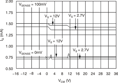
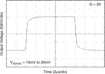
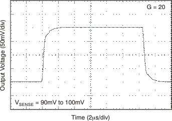
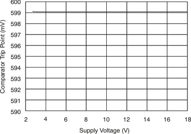
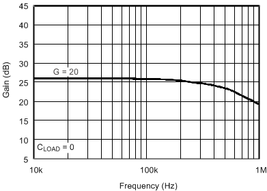
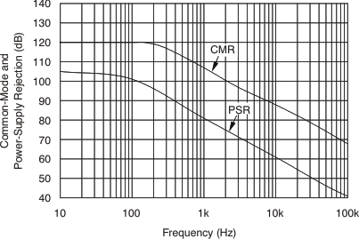
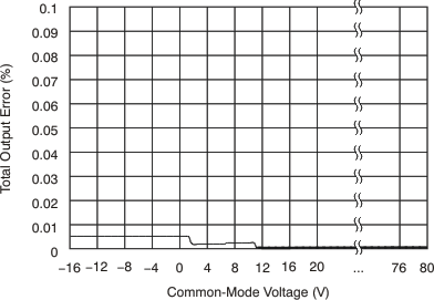
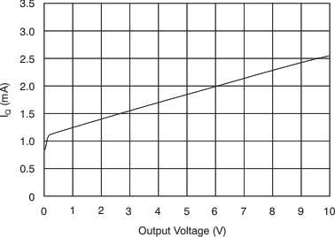
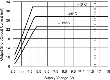
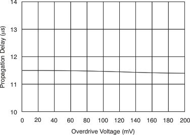
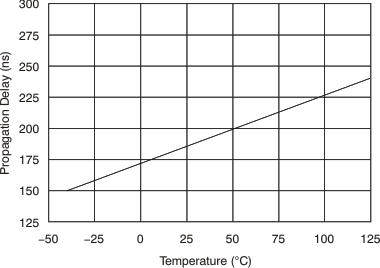
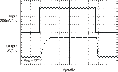
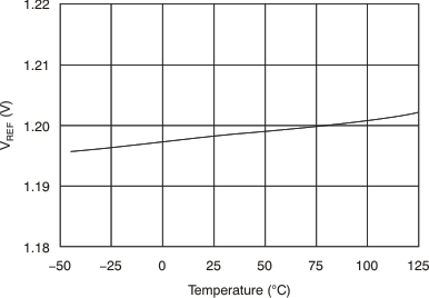
All specifications at TA = +25°C, VS = +12 V, VCM = +12 V, and VSENSE = 100 mV, unless otherwise noted.