SBOS977A March 2019 – May 2021 INA302-Q1 , INA303-Q1
PRODUCTION DATA
- 1 Features
- 2 Applications
- 3 Description
- 4 Revision History
- 5 Pin Configuration and Functions
- 6 Specifications
- 7 Detailed Description
- 8 Application and Implementation
- 9 Power Supply Recommendations
- 10Layout
- 11Device and Documentation Support
- 12Mechanical, Packaging, and Orderable Information
Package Options
Mechanical Data (Package|Pins)
- PW|14
Thermal pad, mechanical data (Package|Pins)
Orderable Information
3 Description
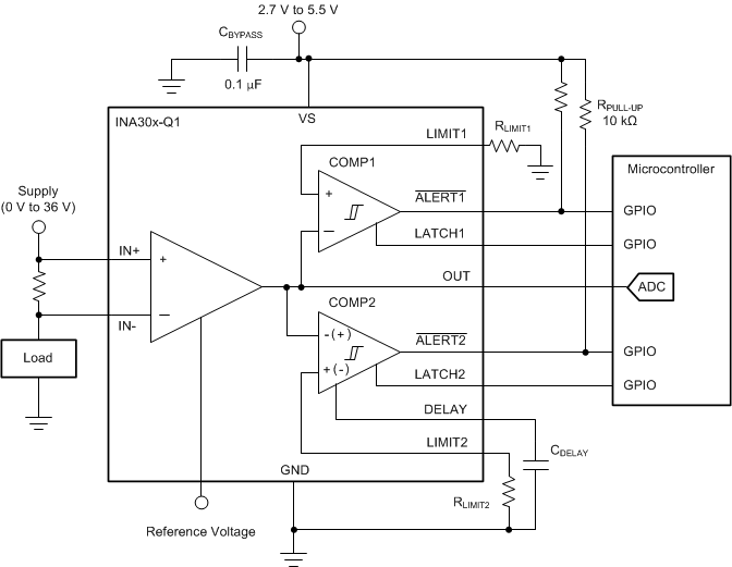
The INA302-Q1 and INA303-Q1 (INA30x-Q1) devices feature a high common-mode, bidirectional, current-sensing amplifier and two high-speed comparators to detect out-of-range current conditions. The INA302-Q1 comparators are configured to detect and respond to overcurrent conditions. The INA303-Q1 comparators are configured to respond to both overcurrent and undercurrent conditions in a windowed configuration. These devices feature an adjustable limit threshold range for each comparator set using an external limit-setting resistor. These current-shunt monitors can measure differential voltage signals on common-mode voltages that can vary from –0.1 V up to +36 V, independent of the supply. In addition, these devices will survive with common-mode voltages as high as 40 V.
The open-drain alert outputs can be configured to operate in either a transparent mode (output status follows the input state), or in a latched mode (alert output is cleared when the latch is reset). The alert response time for comparator 1 is under 1 µs, and the alert response for comparator 2 is set through an external capacitor ranging from 2 µs to 10 s.
These devices operate from a single 2.7-V to 5.5-V supply, drawing a maximum supply current of 950 μA. The devices are specified over the extended operating temperature range of –40°C to +125°C, and are available in a 14-pin TSSOP package.
| PART NUMBER | PACKAGE | BODY SIZE (NOM) |
|---|---|---|
| INA302-Q1 | TSSOP (14) | 4.40 mm × 5.00 mm |
| INA303-Q1 |
 Typical Application