SBAS738A June 2018 – October 2018 ISO224
PRODUCTION DATA.
- 1 Features
- 2 Applications
- 3 Description
- 4 Revision History
- 5 Device Comparison Table
- 6 Pin Configuration and Functions
-
7 Specifications
- 7.1 Absolute Maximum Ratings
- 7.2 ESD Ratings
- 7.3 Recommended Operating Conditions
- 7.4 Thermal Information
- 7.5 Power Ratings
- 7.6 Insulation Specifications
- 7.7 Safety-Related Certifications
- 7.8 Safety Limiting Values
- 7.9 Electrical Characteristics
- 7.10 Switching Characteristics
- 7.11 Insulation Characteristics Curves
- 7.12 Typical Characteristics
- 8 Detailed Description
- 9 Application and Implementation
- 10Power Supply Recommendations
- 11Layout
- 12Device and Documentation Support
- 13Mechanical, Packaging, and Orderable Information
Package Options
Mechanical Data (Package|Pins)
- DWV|8
Thermal pad, mechanical data (Package|Pins)
Orderable Information
8.3.4 Fail-Safe Output
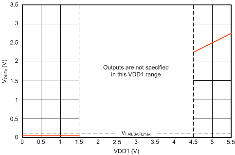
The ISO224 offers a fail-safe output that simplifies diagnostics on system level. The fail-safe output is active when the high-side power supply VDD1 of the device is missing, independent of the input signal at the IN pin. Figure 46 shows that in that case both outputs, OUTP and OUTN, of the device are actively driven close to GND2 (see the VFAILSAFE specification in the Electrical Characteristics table for details). For easy visualization, an example with the input signal VIN = 0 V is shown for the valid VDD1 range of 4.5 V to 5.5 V.
 Figure 46. ISO224 Failsafe Output Behavior With VIN = 0 V
 The ISO224 Fail-Safe Output Feature application report describes an example of a comparator-based circuit that detects the missing high-side supply in a system.