SLLSFX1 September 2024 ISO6163
ADVANCE INFORMATION
- 1
- 1 Features
- 2 Applications
- 3 Description
- 4 Pin Configuration and Functions
-
5 Specifications
- 5.1 Absolute Maximum Ratings
- 5.2 ESD Ratings
- 5.3 Recommended Operating Conditions
- 5.4 Thermal Information
- 5.5 Power Ratings
- 5.6 Insulation Specifications
- 5.7 Safety-Related Certifications
- 5.8 Safety Limiting Values
- 5.9 Electrical Characteristics—5V Supply (±10%)
- 5.10 Supply Current Characteristics—5V Supply (±10%)
- 5.11 Electrical Characteristics—3.3V Supply (±10%)
- 5.12 Supply Current Characteristics—3.3V Supply (±10%)
- 5.13 Electrical Characteristics—2.5V Supply (Minimum)
- 5.14 Supply Current Characteristics—2.5V Supply (Minimum)
- 5.15 Switching Characteristics—5V Supply (±10%)
- 5.16 Switching Characteristics—3.3V Supply (±10%)
- 5.17 Switching Characteristics—2.5V Supply (Minimum)
- 5.18 Insulation Characteristics Curves
- 5.19
Typical Characteristics
- 5.19.1 Typical Characteristics: Supply Current ACTIVE state
- 5.19.2 Typical Characteristics: High-Speed Channels (ACTIVE state)
- 5.19.3 Typical Characteristics: Supply Current STANDBY State
- 5.19.4 Typical Characteristics: Low-Speed Control Channels (ACTIVE and STANDBY States)
- 5.19.5 Typical Characteristics: Undervoltage Threshold
- 6 Parameter Measurement Information
- 7 Detailed Description
- 8 Application and Implementation
- 9 Device and Documentation Support
- 10Revision History
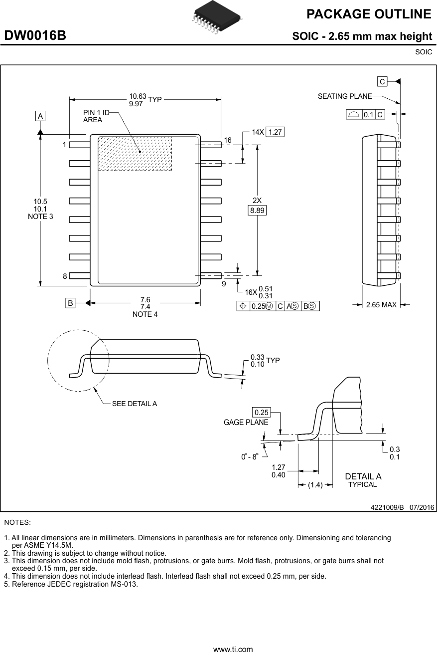
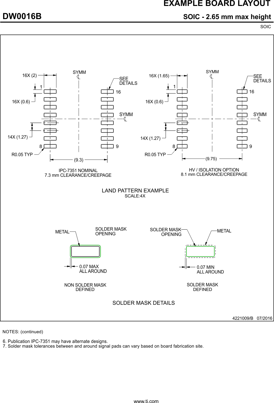
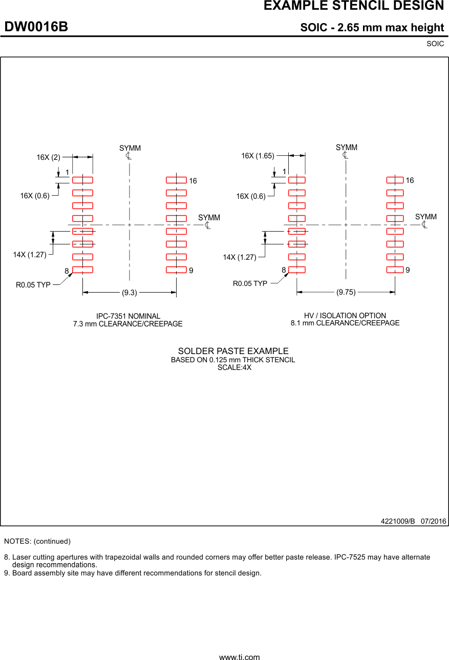
- 11Mechanical, Packaging, and Orderable Information
Refer to the PDF data sheet for device specific package drawings
Mechanical Data (Package|Pins)
- DW|16
Thermal pad, mechanical data (Package|Pins)
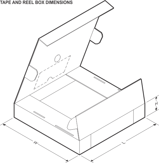
11.2 Tape and Reel Information
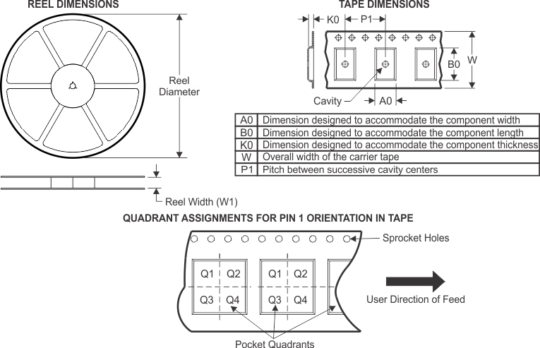
| Device | Package Type |
Package Drawing | Pins | SPQ | Reel Diameter (mm) |
Reel Width W1 (mm) |
A0 (mm) |
B0 (mm) |
K0 (mm) |
P1 (mm) |
W (mm) |
Pin1 Quadrant |
|---|---|---|---|---|---|---|---|---|---|---|---|---|
| ISO6163QDWR | SOIC | DW | 16 | 2000 | 330.0 | 24.4 | 10.9 | 10.7 | 2.7 | 12.0 | 24.0 | Q1 |
| Device | Package Type | Package Drawing | Pins | SPQ | Length (mm) | Width (mm) | Height (mm) |
|---|---|---|---|---|---|---|---|
| ISO6163QDWR | SOIC | DW | 16 | 2000 | 367.0 | 367.0 | 45.0 |