SLLSFF5H January 2020 – May 2022 ISO6720-Q1 , ISO6721-Q1 , ISO6721R-Q1
PRODUCTION DATA
- 1 Features
- 2 Applications
- 3 Description
- 4 Revision History
- 5 Description (continued)
- 6 Pin Configuration and Functions
-
7 Specifications
- 7.1 Absolute Maximum Ratings
- 7.2 ESD Ratings
- 7.3 Recommended Operating Conditions
- 7.4 Thermal Information
- 7.5 Power Ratings
- Insulation Specifications
- 7.6 Safety-Related Certifications
- 7.7 Safety Limiting Values
- Electrical Characteristics—5-V Supply
- 7.8 Supply Current Characteristics—5-V Supply
- 7.9 Electrical Characteristics—3.3-V Supply
- 7.10 Supply Current Characteristics—3.3-V Supply
- 7.11 Electrical Characteristics—2.5-V Supply
- 7.12 Supply Current Characteristics—2.5-V Supply
- Electrical Characteristics—1.8-V Supply
- 7.13 Supply Current Characteristics—1.8-V Supply
- 7.14 Switching Characteristics—5-V Supply
- 7.15 Switching Characteristics—3.3-V Supply
- 7.16 Switching Characteristics—2.5-V Supply
- 7.17 Switching Characteristics—1.8-V Supply
- 7.18 Insulation Characteristics Curves
- 7.19 Typical Characteristics
- 8 Parameter Measurement Information
- 9 Detailed Description
- 10Application and Implementation
- 11Power Supply Recommendations
- 12Layout
- 13Device and Documentation Support
- 14Mechanical, Packaging, and Orderable Information
Package Options
Mechanical Data (Package|Pins)
Thermal pad, mechanical data (Package|Pins)
Orderable Information
3 Description
The ISO672x-Q1 devices are high-performance, dual-channel digital isolators ideal for cost sensitive applications requiring up to 5000 VRMS (DWV package) and 3000 VRMS (D package) isolation ratings per UL 1577. These devices are also certified by VDE, TUV, CSA, and CQC.
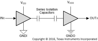
The ISO672x-Q1 devices provide high electromagnetic immunity and low emissions at low power consumption, while isolating CMOS or LVCMOS digital I/Os. Each isolation channel has a logic input and output buffer separated by TI's double capacitive silicon dioxide (SiO2) insulation barrier. The ISO6720-Q1 device has 2 isolation channels with both channels in the same direction. The ISO6721-Q1 device has 2 isolation channels with 1 channel in each direction. In the event of input power or signal loss, the default output is high for devices without suffix F and low for devices with suffix F. See Device Functional Modes section for further details.
| PART NUMBER(1) | PACKAGE | BODY SIZE (NOM) |
|---|---|---|
| ISO6720B-Q1, ISO6720FB-Q1 | D (8) | 4.90 mm x 3.91 mm |
| ISO6721B-Q1, ISO6721FB-Q1 | ||
| ISO6721RB-Q1, ISO6721RFB-Q1 | ||
| ISO6720-Q1, ISO6720F-Q1 | DWV (8) | 5.85 mm x 7.50 mm |
| ISO6721-Q1, ISO6721F-Q1 |
