SLLSEA5C March 2012 – March 2019 ISO7421E-Q1
PRODUCTION DATA.
- 1 Features
- 2 Applications
- 3 Description
- 4 Pin Configuration and Functions
- 5 Electrostatic Discharge Caution
- 6 Absolute Maximum Ratings
- 7 Thermal Information
- 8 Recommended Operating Conditions
- 9 Electrical Characteristics
- 10Switching Characteristics
- 11Electrical Characteristics
- 12Switching Characteristics
- 13Electrical Characteristics
- 14Switching Characteristics
- 15Electrical Characteristics
- 16Switching Characteristics
- 17Parameter Measurement Information
- 18Device Information
- 19Typical Characteristics
- 20Revision History
Package Options
Mechanical Data (Package|Pins)
- DW|16
Thermal pad, mechanical data (Package|Pins)
- DW|16
Orderable Information
3 Description
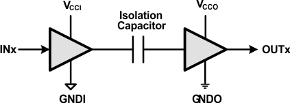
The ISO7421E-Q1 provides double galvanic isolation of up to 2.5 KVrms for 1 minute per UL. This digital isolator has two isolation channels in a bi-directional configuration. Each isolation channel has a logic input and output buffer separated by a silicon oxide (SiO2) insulation barrier. Used in conjunction with isolated power supplies, these devices prevent noise currents on a data bus or other circuits from entering the local ground and interfering with or damaging sensitive circuitry.
The devices have TTL input thresholds and require two supply voltages, 3.3 V or 5 V, or any combination. All inputs are 5-V tolerant when supplied from a 3.3-V supply.
Note: The ISO7421E-Q1 is specified for signaling rates up to 50 Mbps. Due to their fast response time, under most cases, these devices will also transmit data with much shorter pulse widths. Designers should add external filtering to remove spurious signals with input pulse duration < 20 ns if desired.
