SLLSER9E November 2016 – December 2024 ISO7710
PRODUCTION DATA
- 1
- 1 Features
- 2 Applications
- 3 Description
- 4 Pin Configuration and Functions
-
5 Specifications
- 5.1 Absolute Maximum Ratings
- 5.2 ESD Ratings
- 5.3 Recommended Operating Conditions
- 5.4 Thermal Information
- 5.5 Power Ratings
- 5.6 Insulation Specifications
- 5.7 Safety-Related Certifications
- 5.8 Safety Limiting Values
- 5.9 Electrical Characteristics—5-V Supply
- 5.10 Supply Current Characteristics—5-V Supply
- 5.11 Electrical Characteristics—3.3-V Supply
- 5.12 Supply Current Characteristics—3.3-V Supply
- 5.13 Electrical Characteristics—2.5-V Supply
- 5.14 Supply Current Characteristics—2.5-V Supply
- 5.15 Switching Characteristics—5-V Supply
- 5.16 Switching Characteristics—3.3-V Supply
- 5.17 Switching Characteristics—2.5-V Supply
- 5.18 Insulation Characteristics Curves
- 5.19 Typical Characteristics
- 6 Parameter Measurement Information
- 7 Detailed Description
- 8 Application and Implementation
- 9 Device and Documentation Support
- 10Revision History
- 11Mechanical, Packaging, and Orderable Information
Package Options
Refer to the PDF data sheet for device specific package drawings
Mechanical Data (Package|Pins)
- D|8
- DW|16
Thermal pad, mechanical data (Package|Pins)
Orderable Information
3 Description
The ISO7710 device is a high-performance, single-channel digital isolator with 5000VRMS (DW package) and 3000VRMS (D package) isolation ratings per UL 1577. This device is also certified by VDE, TUV, CSA, and CQC.
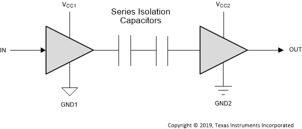
The ISO7710 device provides high electromagnetic immunity and low emissions at low power consumption, while isolating CMOS or LVCMOS digital I/Os. The isolation channel has a logic input and output buffer separated by a double capacitive silicon dioxide (SiO2) insulation barrier. In the event of input power or signal loss, default output is high for a device without suffix F and low for a device with suffix F. See the Device Functional Modes section for further details.
Used in conjunction with isolated power supplies, the device helps prevent noise currents on data buses, such as RS-485, RS-232, and CAN , or other circuits from entering the local ground and interfering with or damaging sensitive circuitry. Through innovative chip design and layout techniques, the electromagnetic compatibility of the ISO7710 device has been significantly enhanced to ease system-level ESD, EFT, surge, and emissions compliance. The ISO7710 device is available in 16-pin SOIC wide-body (DW) and 8-pin SOIC narrow-body (D) packages.
| PART NUMBER | PACKAGE(1) | PACKAGE SIZE(2) | BODY SIZE (NOM) |
|---|---|---|---|
| ISO7710 | SOIC (D) | 4.90mm × 6mm | 4.90mm × 3.91mm |
| SOIC (DW) | 10.30mm × 10.30mm | 10.30mm × 7.50mm |
 Simplified Schematic