SLLSER9E November   2016  – December 2024 ISO7710

PRODUCTION DATA  

  1.   1
  2. Features
  3. Applications
  4. Description
  5. Pin Configuration and Functions
    1.     Pin Functions
  6. Specifications
    1. 5.1  Absolute Maximum Ratings
    2. 5.2  ESD Ratings
    3. 5.3  Recommended Operating Conditions
    4. 5.4  Thermal Information
    5. 5.5  Power Ratings
    6. 5.6  Insulation Specifications
    7. 5.7  Safety-Related Certifications
    8. 5.8  Safety Limiting Values
    9. 5.9  Electrical Characteristics—5-V Supply
    10. 5.10 Supply Current Characteristics—5-V Supply
    11. 5.11 Electrical Characteristics—3.3-V Supply
    12. 5.12 Supply Current Characteristics—3.3-V Supply
    13. 5.13 Electrical Characteristics—2.5-V Supply 
    14. 5.14 Supply Current Characteristics—2.5-V Supply
    15. 5.15 Switching Characteristics—5-V Supply
    16. 5.16 Switching Characteristics—3.3-V Supply
    17. 5.17 Switching Characteristics—2.5-V Supply
    18. 5.18 Insulation Characteristics Curves
    19. 5.19 Typical Characteristics
  7. Parameter Measurement Information
  8. Detailed Description
    1. 7.1 Overview
    2. 7.2 Functional Block Diagram
    3. 7.3 Feature Description
      1. 7.3.1 Electromagnetic Compatibility (EMC) Considerations
    4. 7.4 Device Functional Modes
      1. 7.4.1 Device I/O Schematics
  9. Application and Implementation
    1. 8.1 Application Information
    2. 8.2 Typical Application
      1. 8.2.1 Design Requirements
      2. 8.2.2 Detailed Design Procedure
      3. 8.2.3 Application Curve
        1. 8.2.3.1 Insulation Lifetime
    3. 8.3 Power Supply Recommendations
    4. 8.4 Layout
      1. 8.4.1 Layout Guidelines
        1. 8.4.1.1 PCB Material
      2. 8.4.2 Layout Example
  10. Device and Documentation Support
    1. 9.1 Documentation Support
      1. 9.1.1 Related Documentation
    2. 9.2 Receiving Notification of Documentation Updates
    3. 9.3 Support Resources
    4. 9.4 Trademarks
    5. 9.5 Electrostatic Discharge Caution
    6. 9.6 Glossary
  11. 10Revision History
  12. 11Mechanical, Packaging, and Orderable Information

Package Options

Refer to the PDF data sheet for device specific package drawings

Mechanical Data (Package|Pins)
  • D|8
  • DW|16
Thermal pad, mechanical data (Package|Pins)
Orderable Information

Typical Characteristics

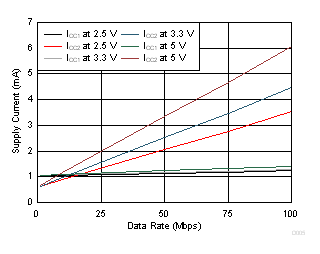
ISO7710 ISO7710 Supply Current vs Data Rate (With 15 pF Load)
TA = 25°CCL = 15 pF
Figure 5-5 ISO7710 Supply Current vs Data Rate (With 15 pF Load)
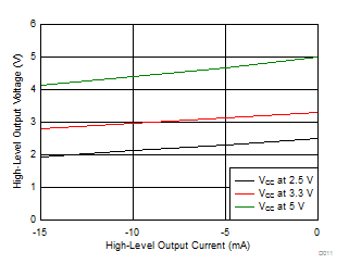
ISO7710 High-Level Output Voltage vs High-level  Output Current
TA = 25°C
Figure 5-7 High-Level Output Voltage vs High-level Output Current
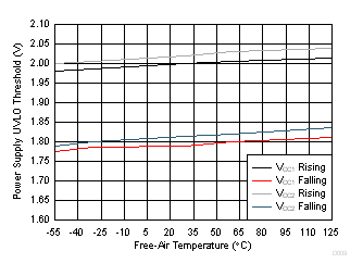
ISO7710 Power Supply Undervoltage Threshold vs  Free-Air Temperature
Figure 5-9 Power Supply Undervoltage Threshold vs Free-Air Temperature
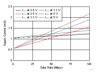
ISO7710 ISO7710 Supply Current vs Data Rate (With No Load)
TA = 25°CCL = No Load
Figure 5-6 ISO7710 Supply Current vs Data Rate (With No Load)
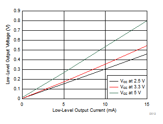
ISO7710 Low-Level Output Voltage vs Low-Level  Output Current
TA = 25°C
Figure 5-8 Low-Level Output Voltage vs Low-Level Output Current
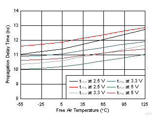
ISO7710 Propagation Delay Time vs Free-Air Temperature
Figure 5-10 Propagation Delay Time vs Free-Air Temperature