SLLSEM2H November 2014 – November 2024 ISO7821
PRODUCTION DATA
- 1
- 1 Features
- 2 Applications
- 3 Description
- 4 Pin Configuration and Functions
-
5 Specifications
- 5.1 Absolute Maximum Ratings
- 5.2 ESD Ratings
- 5.3 Recommended Operating Conditions
- 5.4 Thermal Information
- 5.5 Power Dissipation Characteristics
- 5.6 Electrical Characteristics, 5 V
- 5.7 Electrical Characteristics, 3.3 V
- 5.8 Electrical Characteristics, 2.5 V
- 5.9 Power Ratings
- 5.10 Insulation Specifications
- 5.11 Safety-Related Certifications
- 5.12 Safety Limiting Values
- 5.13 Switching Characteristics, 5 V
- 5.14 Switching Characteristics, 3.3 V
- 5.15 Switching Characteristics, 2.5 V
- 5.16 Typical Characteristics
- 6 Parameter Measurement Information
- 7 Detailed Description
- 8 Application and Implementation
- 9 Device and Documentation Support
- 10Revision History
- 11Mechanical, Packaging, and Orderable Information
Package Options
Refer to the PDF data sheet for device specific package drawings
Mechanical Data (Package|Pins)
- DWW|16
- DW|16
Thermal pad, mechanical data (Package|Pins)
Orderable Information
5.12 Safety Limiting Values
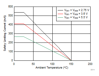
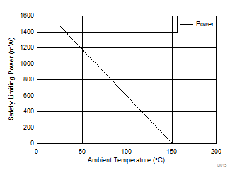
Safety limiting intends to prevent potential damage to the isolation barrier upon failure of input or output circuitry. A failure of the I/O can allow low resistance to ground or the supply and, without current limiting, dissipate sufficient power to overheat the die and damage the isolation barrier potentially leading to secondary system failures.
| PARAMETER | TEST CONDITIONS | MIN | TYP | MAX | UNIT | |
|---|---|---|---|---|---|---|
| IS | Safety input, output, or supply current for DW-16 package and DWW-16 Packages | RθJA = 84.7°C/W, VI = 5.5 V, TJ = 150°C, TA = 25°C | 268 | mA | ||
| RθJA = 84.7°C/W, VI = 3.6 V, TJ = 150°C, TA = 25°C | 410 | |||||
| RθJA = 84.7°C/W, VI = 2.75 V, TJ = 150°C, TA = 25°C | 537 | |||||
| PS | Safety input, output, or total power | RθJA = 84.7°C/W, TJ = 150°C, TA = 25°C | 1476 | mW | ||
| TS | Maximum safety temperature | 150 | °C | |||
The maximum safety temperature is the maximum junction temperature specified for the device. The power dissipation and junction-to-air thermal impedance of the device installed in the application hardware determines the junction temperature. The assumed junction-to-air thermal resistance in the Section 5.4 is that of a device installed on a High-K test board for Leaded Surface Mount Packages. The power is the recommended maximum input voltage times the current. The junction temperature is then the ambient temperature plus the power times the junction-to-air thermal resistance.
 Figure 5-1 Thermal Derating Curve for Safety Limiting Current per VDE
 Figure 5-2 Thermal Derating Curve for Safety Limiting Power per VDE