SLLSEP8B July 2015 – June 2016 ISO7831
PRODUCTION DATA.
- 1 Features
- 2 Applications
- 3 Description
- 4 Revision History
- 5 Pin Configuration and Functions
-
6 Specifications
- 6.1 Absolute Maximum Ratings
- 6.2 ESD Ratings
- 6.3 Recommended Operating Conditions
- 6.4 Thermal Information
- 6.5 Power Rating
- 6.6 Insulation Characteristics
- 6.7 Regulatory Information
- 6.8 Safety Limiting Values
- 6.9 Electrical Characteristics—5-V Supply
- 6.10 Supply Current Characteristics—5-V Supply
- 6.11 Electrical Characteristics—3.3-V Supply
- 6.12 Supply Current Characteristics—3.3-V Supply
- 6.13 Electrical Characteristics—2.5-V Supply
- 6.14 Supply Current Characteristics—2.5-V Supply
- 6.15 Switching Characteristics—5-V Supply
- 6.16 Switching Characteristics—3.3-V Supply
- 6.17 Switching Characteristics—2.5-V Supply
- 6.18 Insulation Characteristics Curves
- 6.19 Typical Characteristics
- 7 Parameter Measurement Information
- 8 Detailed Description
- 9 Application and Implementation
- 10Power Supply Recommendations
- 11Layout
- 12Device and Documentation Support
- 13Mechanical, Packaging, and Orderable Information
Package Options
Refer to the PDF data sheet for device specific package drawings
Mechanical Data (Package|Pins)
- DWW|16
- DW|16
Thermal pad, mechanical data (Package|Pins)
Orderable Information
9 Application and Implementation
NOTE
Information in the following applications sections is not part of the TI component specification, and TI does not warrant its accuracy or completeness. TI’s customers are responsible for determining suitability of components for their purposes. Customers should validate and test their design implementation to confirm system functionality.
9.1 Application Information
The ISO7831x device is a high-performance, triple-channel digital isolator with 5.7-kVRMS isolation voltage. The device comes with enable pins on each side which can be used to put the respective outputs in high impedance for multi-master driving applications and reduce power consumption. The ISO7831x device uses single-ended CMOS-logic switching technology. The supply voltage range is from 2.25 V to 5.5 V for both supplies, VCC1 and VCC2. When designing with digital isolators, keep in mind that because of the single-ended design structure, digital isolators do not conform to any specific interface standard and are only intended for isolating single-ended CMOS or TTL digital signal lines. The isolator is typically placed between the data controller (that is, μC or UART), and a data converter or a line transceiver, regardless of the interface type or standard.
9.2 Typical Application
Figure 20 shows the isolated RS-485 interface application circuit.
 Figure 20. Isolated RS-485 Circuit
9.2.1 Design Requirements
For this design example, use the parameters listed in Table 3.
Table 3. Design Parameters
| PARAMETER | VALUE |
|---|---|
| Supply voltage | 2.25 to 5.5 V |
| Decoupling capacitor between VCC1 and GND1 | 0.1 µF |
| Decoupling capacitor from VCC2 and GND2 | 0.1 µF |
9.2.2 Detailed Design Procedure
Unlike optocouplers, which require external components to improve performance, provide bias, or limit current, ISO7831x only requires two external bypass capacitors to operate.
 Figure 21. Typical ISO7831 Circuit Hook-up
9.2.3 Application Curve
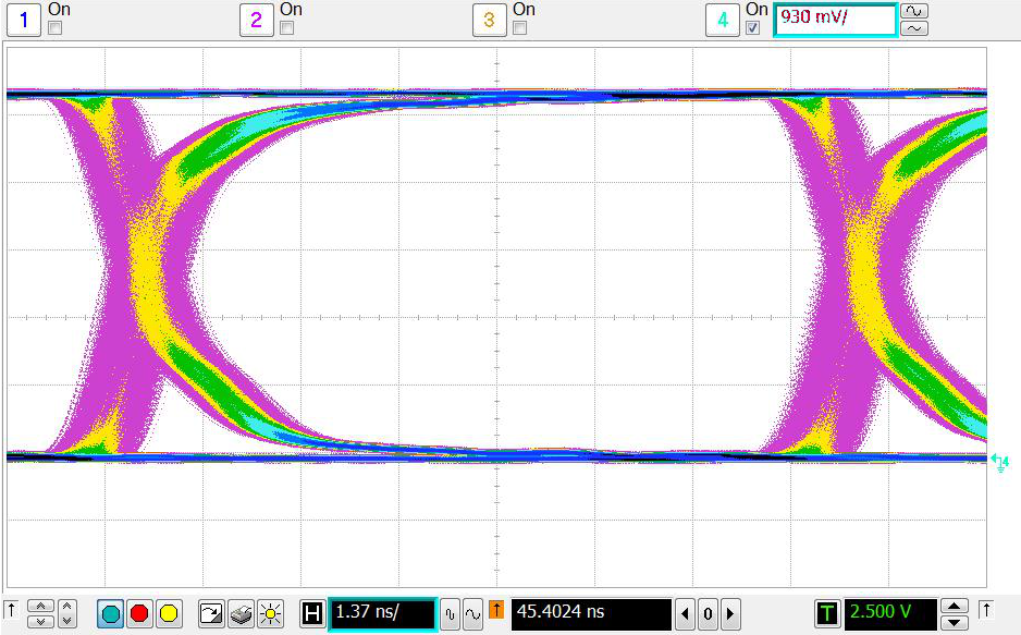
The following typical eye diagram of the ISO7831x device indicates low jitter and wide open eye at the maximum data rate of 100 Mbps.
 Figure 22. Eye Diagram at 100 Mbps PRBS, 5 V and 25°C