SLLSEN2B July 2015 – April 2016 ISO7840
PRODUCTION DATA.
- 1 Features
- 2 Applications
- 3 Description
- 4 Revision History
- 5 Pin Configuration and Functions
-
6 Specifications
- 6.1 Absolute Maximum Ratings
- 6.2 ESD Ratings
- 6.3 Recommended Operating Conditions
- 6.4 Thermal Information
- 6.5 Power Ratings
- 6.6 Insulation Specifications
- 6.7 Safety-Related Certifications
- 6.8 Safety Limiting Values
- 6.9 Electrical Characteristics—5-V Supply
- 6.10 Supply Characteristics—5-V Supply
- 6.11 Electrical Characteristics—3.3-V Supply
- 6.12 Supply Current Characteristics—3.3-V Supply
- 6.13 Electrical Characteristics—2.5-V Supply
- 6.14 Supply Current Characteristics—2.5-V Supply
- 6.15 Switching Characteristics—5-V Supply
- 6.16 Switching Characteristics—3.3-V Supply
- 6.17 Switching Characteristics—2.5-V Supply
- 6.18 Insulation Characteristics Curves
- 6.19 Typical Characteristics
- 7 Parameter Measurement Information
- 8 Detailed Description
- 9 Application and Implementation
- 10Power Supply Recommendations
- 11Layout
- 12Device and Documentation Support
- 13Mechanical, Packaging, and Orderable Information
Package Options
Refer to the PDF data sheet for device specific package drawings
Mechanical Data (Package|Pins)
- DWW|16
- DW|16
Thermal pad, mechanical data (Package|Pins)
Orderable Information
1 Features
- Signaling Rate: Up to 100 Mbps
- Wide Supply Range: 2.25 V to 5.5 V
- 2.25-V to 5.5-V Level Translation
- Wide Temperature Range: –55°C to +125°C
- Low-Power Consumption, Typical 1.7 mA per Channel at 1 Mbps
- Low Propagation Delay: 11 ns Typical
(5-V Supplies) - Industry leading CMTI (Min): ±100 kV/μs
- Robust Electromagnetic Compatibility (EMC)
- System-Level ESD, EFT, and Surge Immunity
- Low Emissions
- Isolation Barrier Life: >40 Years
- Wide Body SOIC-16 Package and Extra-Wide Body SOIC-16 Package Options
- Safety and Regulatory Approvals:
- 8000-VPK Reinforced Isolation per DIN V VDE V 0884-10 (VDE V 0884-10):2006-12
- 5.7-kVRMS Isolation for 1 Minute per UL 1577
- CSA Component Acceptance Notice 5A, IEC 60950-1 and IEC 60601-1 End Equipment Standards
- CQC Certification per GB4943.1-2011
- TUV Certification per EN 61010-1 and EN 60950-1
- All DW Package Certifications Complete; DWW Package Certifications Complete per UL, VDE, TUV and Planned for CSA and CQC
2 Applications
- Industrial Automation
- Motor Control
- Power Supplies
- Solar Inverters
- Medical Equipment
- Hybrid Electric Vehicles
3 Description
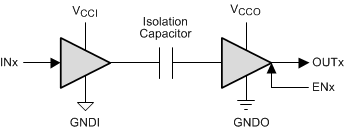
The ISO7840x device is a high-performance, quad-channel digital isolator with a 8000-VPK isolation voltage. This device has reinforced isolation certifications according to VDE, CSA, CQC, and TUV. The isolator provides high electromagnetic immunity and low emissions at low-power consumption, while isolating CMOS or LVCMOS digital I/Os. Each isolation channel has a logic input and output buffer separated by a silicon-dioxide (SiO2) insulation barrier.
This device comes with enable pins that can be used to put the respective outputs in high impedance for multi-master driving applications and to reduce power consumption. The ISO7840 device has four forward and zero reverse-direction channels. If the input power or signal is lost, the default output is high for the ISO7840 device and low for the ISO7840F device. See the Device Functional Modes section for further details.
Used in conjunction with isolated power supplies, this device helps prevent noise currents on a data bus or other circuits from entering the local ground and interfering with or damaging sensitive circuitry. Through innovative chip design and layout techniques, electromagnetic compatibility of the ISO7840 device has been significantly enhanced to ease system-level ESD, EFT, surge, and emissions compliance.
The ISO7840 device is available in 16-pin SOIC wide-body (DW) and extra-wide body (DWW) packages.
Device Information(1)
| PART NUMBER | PACKAGE | BODY SIZE (NOM) |
|---|---|---|
| ISO7840
ISO7840F |
DW (16) | 10.30 mm × 7.50 mm |
| DWW (16) | 10.30 mm × 14.0 mm |
- For all available packages, see the orderable addendum at the end of the data sheet.
Simplified Schematic

4 Revision History
Changes from A Revision (March 2016) to B Revision
- Added Features 2.25 V to 5.5 V Level TranslationGo
- Changed the number of years for the isolation barrier life in the Features section Go
- VDE certification is now complete Go
- Changed the input-to-output test voltage parameter to apparent charge in the Insulation Specifications Go
- Changed VCCO to VCCI for the minimum value of the input threshold voltage hysteresis parameter in all electrical characteristics tablesGo
- Added VCM to the test condition of the common-mode transient immunity parameter in all electrical characteristics tablesGo
- Added the lifetime projection graphs for DW and DWW packages to the Safety Limiting Values section Go
Changes from * Revision (July 2015) to A Revision
- Changed Features From: Industry leading CMTI To: Industry leading CMTI (MIN) Go
- Changed the Safety and Regulatory Approvals list of FeaturesGo
- Added Features "TUV Certification per EN 61010-1 and EN 60950-1"Go
- Changed text in the first paragraph of the Description From: "certifications according to VDE, CSA, and CQC". To: "certifications according to VDE, CSA, CQC, and TUV." Go
- Added the DWW pinout imageGo
- Added the DWW package to the Thermal Information Go
- Changed Package Insulation and Safety-Related Specifications, added the 16-DWW Package informationGo
- Added the DWW package information, added "Climatic category", and deleted Note 1 in Insulation Characteristics Go
- Added Note 1 to Insulation Characteristics Go
- Changed IEC 60664-1 Ratings Table Go
- Added the TUV and DWW package information to the Regulatory Information section and Regulatory Information. Deleted Note 1 in Regulatory InformationGo
- Changed the Supply Current section of Supply Characteristics—5-V SupplyGo
- Changed the Supply Current section of Supply Current Characteristics—3.3-V SupplyGo
- Changed the Supply Current section ofSupply Current Characteristics—2.5-V Supply Go
- Changed Device I/O Schematics Go