SLLSF40B November 2017 – September 2019 ISOW7821
PRODUCTION DATA.
- 1 Features
- 2 Applications
- 3 Description
- 4 Revision History
- 5 Description (continued)
- 6 Pin Configuration and Functions
-
7 Specifications
- 7.1 Absolute Maximum Ratings
- 7.2 ESD Ratings
- 7.3 Recommended Operating Conditions
- 7.4 Thermal Information
- 7.5 Power Ratings
- 7.6 Insulation Specifications
- 7.7 Safety-Related Certifications
- 7.8 Safety Limiting Values
- 7.9 Electrical Characteristics—5-V Input, 5-V Output
- 7.10 Supply Current Characteristics—5-V Input, 5-V Output
- 7.11 Electrical Characteristics—5-V Input, 3.3-V Output
- 7.12 Supply Current Characteristics—5-V Input, 3.3-V Output
- 7.13 Electrical Characteristics—3.3-V Input, 3.3-V Output
- 7.14 Supply Current Characteristics—3.3-V Input, 3.3-V Output
- 7.15 Switching Characteristics—5-V Input, 5-V Output
- 7.16 Switching Characteristics—5-V Input, 3.3-V Output
- 7.17 Switching Characteristics—3.3-V Input, 3.3-V Output
- 7.18 Insulation Characteristics Curves
- 7.19 Typical Characteristics
- 8 Parameter Measurement Information
- 9 Detailed Description
- 10Application and Implementation
- 11Power Supply Recommendations
- 12Layout
- 13Device and Documentation Support
- 14Mechanical, Packaging, and Orderable Information
Package Options
Mechanical Data (Package|Pins)
- DWE|16
Thermal pad, mechanical data (Package|Pins)
Orderable Information
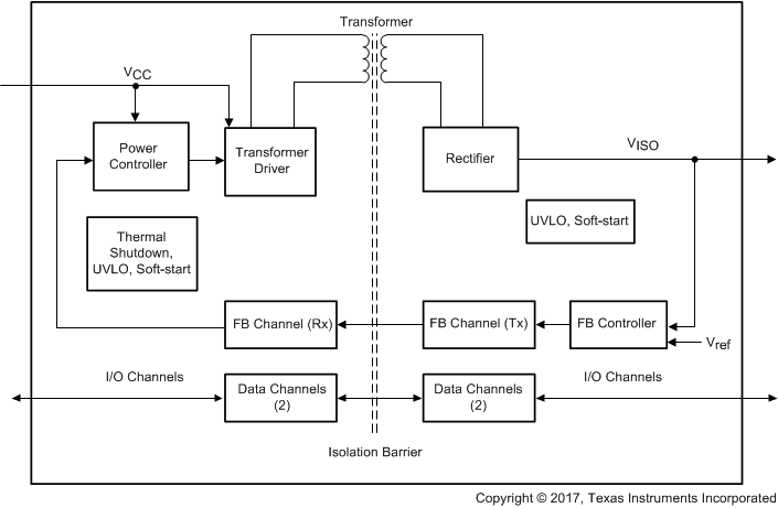
9.2 Functional Block Diagram
 Figure 26. ISOW7821 Block Diagram
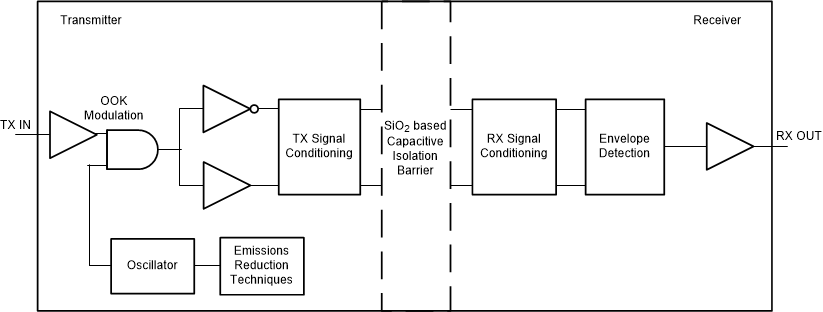
  Figure 27. Conceptual Block Diagram of a Capacitive Data Channel
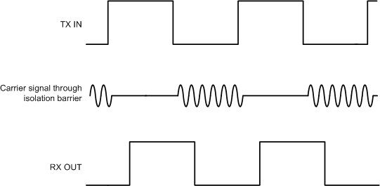
 Figure 28 shows a conceptual detail of how the OOK scheme works.
 Figure 28. On-Off Keying (OOK) Based Modulation Scheme