SLLSEY2G March   2017  – August 2021 ISOW7840 , ISOW7841 , ISOW7842 , ISOW7843 , ISOW7844

PRODUCTION DATA  

  1. Features
  2. Applications
  3. Description
  4. Revision History
  5. Description (continued)
  6. Pin Configuration and Functions
    1.     Pin Functions
  7. Specifications
    1. 7.1  Absolute Maximum Ratings
    2. 7.2  ESD Ratings
    3. 7.3  Recommended Operating Conditions
    4. 7.4  Thermal Information
    5. 7.5  Power Ratings
    6. 7.6  Insulation Specifications
    7. 7.7  Safety-Related Certifications
    8. 7.8  Safety Limiting Values
    9. 7.9  Electrical Characteristics—5-V Input, 5-V Output
    10. 7.10 Supply Current Characteristics—5-V Input, 5-V Output
    11. 7.11 Electrical Characteristics—3.3-V Input, 5-V Output
    12. 7.12 Supply Current Characteristics—3.3-V Input, 5-V Output
    13. 7.13 Electrical Characteristics—5-V Input, 3.3-V Output
    14. 7.14 Supply Current Characteristics—5-V Input, 3.3-V Output
    15. 7.15 Electrical Characteristics—3.3-V Input, 3.3-V Output
    16. 7.16 Supply Current Characteristics—3.3-V Input, 3.3-V Output
    17. 7.17 Switching Characteristics—5-V Input, 5-V Output
    18. 7.18 Switching Characteristics—3.3-V Input, 5-V Output
    19. 7.19 Switching Characteristics—5-V Input, 3.3-V Output
    20. 7.20 Switching Characteristics—3.3-V Input, 3.3-V Output
    21. 7.21 Insulation Characteristics Curves
    22. 7.22 Typical Characteristics
  8. Parameter Measurement Information
  9. Detailed Description
    1. 9.1 Overview
    2. 9.2 Functional Block Diagram
    3. 9.3 Feature Description
      1. 9.3.1 Electromagnetic Compatibility (EMC) Considerations
      2. 9.3.2 Power-Up and Power-Down Behavior
      3. 9.3.3 Current Limit, Thermal Overload Protection
    4. 9.4 Device Functional Modes
      1. 9.4.1 Device I/O Schematics
  10. 10Application and Implementation
    1. 10.1 Application Information
    2. 10.2 Typical Application
      1. 10.2.1 Design Requirements
      2. 10.2.2 Detailed Design Procedure
      3. 10.2.3 Application Curve
        1. 10.2.3.1 Insulation Lifetime
  11. 11Power Supply Recommendations
  12. 12Layout
    1. 12.1 Layout Guidelines
      1. 12.1.1 PCB Material
    2. 12.2 Layout Example
  13. 13Device and Documentation Support
    1. 13.1 Device Support
      1. 13.1.1 Development Support
    2. 13.2 Documentation Support
      1. 13.2.1 Related Documentation
    3. 13.3 Related Links
    4. 13.4 Receiving Notification of Documentation Updates
    5. 13.5 Support Resources
    6. 13.6 Trademarks
    7. 13.7 Electrostatic Discharge Caution
    8. 13.8 Glossary
  14. 14Mechanical, Packaging, and Orderable Information

Package Options

Mechanical Data (Package|Pins)
Thermal pad, mechanical data (Package|Pins)
Orderable Information

Typical Characteristics

GUID-120C6C80-CC8C-4AAC-A071-7A78D2A36938-low.gif
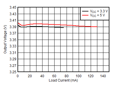
VISO = 3.3 VTA = 25°C
Figure 7-3 Isolated Supply Voltage (VISO) vs Load Current (IISO)
GUID-768A8BE2-F9D5-4F4F-9813-9A6CD167C468-low.gif
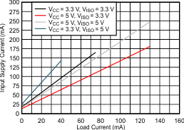
TA = 25°C
Figure 7-5 ISOW7841 Supply Current (ICC) vs Load Current (IISO)
GUID-3A698A4F-9E43-406E-84D8-4C277BB58DC8-low.gif
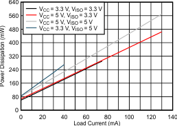
TA = 25°C
Figure 7-7 ISOW7841 Power Dissipation vs Load Current (IISO)
GUID-01FD990F-B399-4F40-8F89-51B5E1E2816F-low.gif
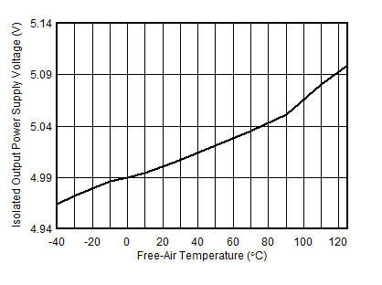
No IISO loadVCC = 5 VVISO = 5 V
Figure 7-9 5-V Isolated Supply Voltage (VISO) vs Free-Air Temperature
GUID-94B8F9D4-02A1-4D4B-B742-0E1453D1844C-low.gif
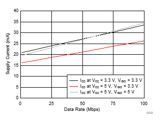
CL = 15 pFTA = 25°CNo IISO load
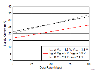
Figure 7-11 ISOW7840 Supply Current vs Data Rate
GUID-F08B5A63-BCC2-4D28-A9E6-613BF753B7F9-low.gif
CL = 15 pF TA = 25°C No IISO load
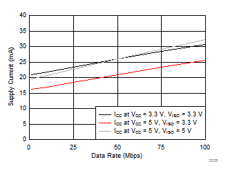
Figure 7-13 ISOW7841 Supply Current vs Data Rate
GUID-9D858161-A676-41C8-9CDC-FE91FC652941-low.gif
CL = 15 pFTA = 25°CNo IISO load
Figure 7-15 ISOW7842 Supply Current vs Data Rate
GUID-1FC9DDF8-8E12-431A-A814-27EB15D6D7A0-low.gif
CL = 15 pFTA = 25°CNo IISO load
Figure 7-17 ISOW7843 Supply Current vs Data Rate
GUID-471E34B3-A575-4202-9936-0320D3BAB44E-low.gif
CL = 15 pFTA = 25°CNo IISO load
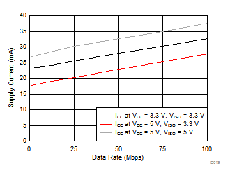
Figure 7-19 ISOW7844 Supply Current vs Data Rate
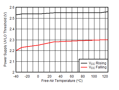
GUID-E08E5E98-2A25-4D2D-AC63-389F19FA7945-low.gifFigure 7-21 Power-Supply Undervoltage Threshold vs Free Air Temperature
GUID-9BD0B9B3-A384-4D49-AE33-CB0B63FB2FA0-low.gif
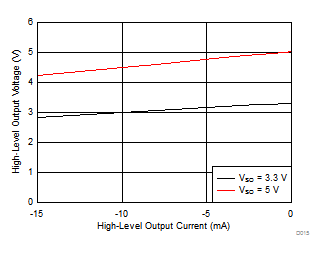
TA = 25°C
Figure 7-23 High-Level Output Voltage vs High-Level Output Current
GUID-E1C5ECE3-9B45-4605-B45C-0A8EB8C853FB-low.gif
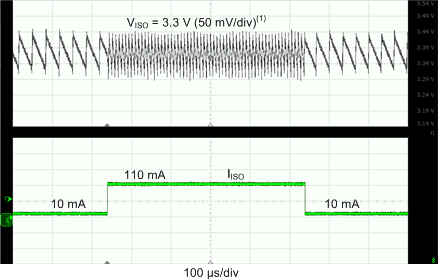
VCC = 5 VVISO = 3.3 V
Negligible undershoot and overshoot because of load transient
Figure 7-25 10-mA to 110-mA Load Transient Response
GUID-83B2BC24-6751-4377-AEA3-7A894B12E28C-low.gif
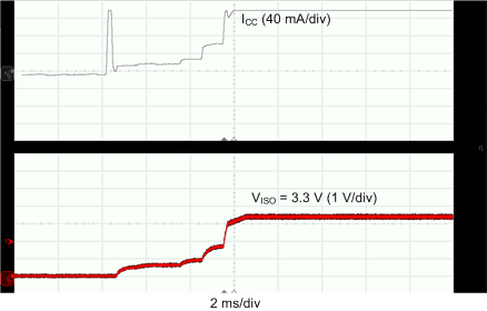
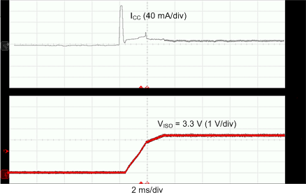
VCC = 5 VVISO = 3.3 V
Input current spike is because of charging the input supply decoupling capacitor
Figure 7-27 Soft Start at 120-mA Load
GUID-AEC6910A-9F19-4360-8DB6-366BDBCD906D-low.gif
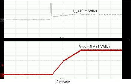
VCC = 5 VVISO = 5 V
Input current spike is because of charging the input supply decoupling capacitor
Figure 7-29 Soft Start at 130-mA Load
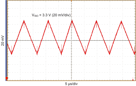
GUID-C58145EB-4443-4D71-841F-9193BFA83234-low.gif
VCC = 5 VVISO = 3.3 V
Figure 7-31 VISO Ripple Voltage at 130 mA
GUID-D45C2E44-5FC8-45DE-8A54-BD104757345A-low.gif
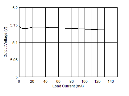
VISO = 5 VTA = 25°C
Figure 7-4 Isolated Supply Voltage (VISO) vs Load Current (IISO)
GUID-D33A026B-DD48-4929-809B-EA2FD4042C83-low.gif
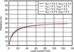
TA = 25°C
Figure 7-6 ISOW7841 Efficiency vs Load Current (IISO)
GUID-98AC7375-A806-4967-AF07-EED57E73070C-low.gif
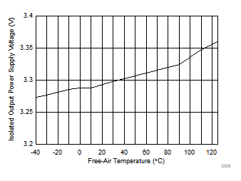
No IISO loadVCC = 5 VVISO = 3.3 V
Figure 7-8 3.3-V Isolated Supply Voltage (VISO) vs Free-Air Temperature
GUID-ECA0C149-12BF-4F67-AEE8-C316BDBAAA2B-low.gif
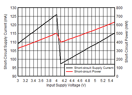
VISO shorted to GND2 TA = 25°C
Figure 7-10 Short-Circuit Supply Current (ICC) and Power (P) vs Supply Voltage (VCC)
GUID-A22DA6D4-105E-41BA-A608-F20C29ACB62F-low.gif
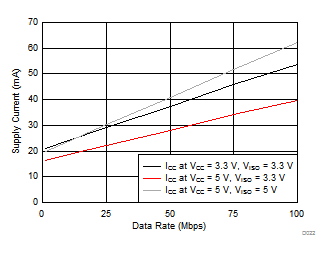
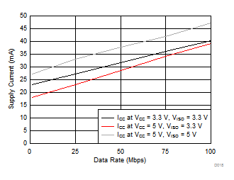
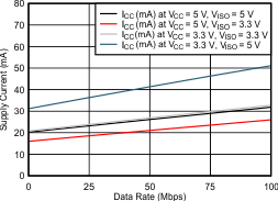
CL = no loadTA = 25°CNo IISO load
Figure 7-12 ISOW7840 Supply Current vs Data Rate
GUID-4FC706B8-7DD8-46AC-90B5-DC7E63D2C1BB-low.gif
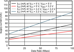
CL = no load TA = 25°C No IISO load
Figure 7-14 ISOW7841 Supply Current vs Data Rate
GUID-3F8D51EC-DC38-4ED5-9928-3D66E7C33101-low.gif
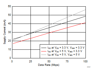
CL = no loadTA = 25°CNo IISO load
Figure 7-16 ISOW7842 Supply Current vs Data Rate
GUID-74AFC8B0-778E-4FB9-97E9-20FBBEC35224-low.gif
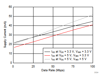
CL = no loadTA = 25°CNo IISO load
Figure 7-18 ISOW7843 Supply Current vs Data Rate
GUID-C1D05661-3F38-48E3-8BDD-120D5AE33096-low.gif
CL = no loadTA = 25°CNo IISO load
Figure 7-20 ISOW7844 Supply Current vs Data Rate
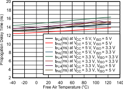
GUID-5D02FC56-B762-46E5-9926-4553A65C02CB-low.gifFigure 7-22 Propagation Delay Time vs Free-Air Temperature
GUID-070A60E3-E62B-4A2E-BB42-95D5411870A2-low.gif
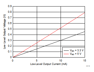
TA = 25°C
Figure 7-24 Low-Level Output Voltage vs Low-Level Output Current
GUID-58ED756F-6B17-4B5F-BB72-4D12B4D25215-low.gif
VCC = 5 VVISO = 3.3 V
Current spike is because of charging the input supply capacitor
Figure 7-26 Soft Start at 10-mA Load
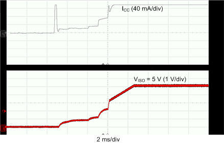
GUID-34A3A3C8-1424-422D-83A2-F7307E6AA907-low.gif
VCC = 5 VVISO = 5 V
Input current spike is because of charging the input supply decoupling capacitor
Figure 7-28 Soft Start at 10-mA Load
GUID-0C8BB663-E42D-4E63-ABAD-D898999EF006-low.gif
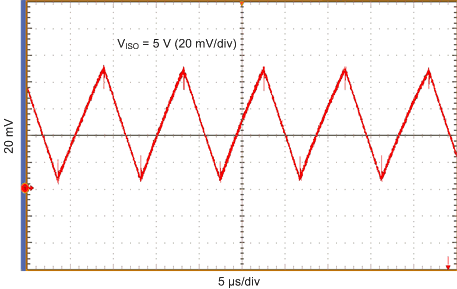
VCC = 5 VVISO = 5 V
Figure 7-30 VISO Ripple Voltage at 130 mA