SLLSEY2G March 2017 – August 2021 ISOW7840 , ISOW7841 , ISOW7842 , ISOW7843 , ISOW7844
PRODUCTION DATA
- 1 Features
- 2 Applications
- 3 Description
- 4 Revision History
- 5 Description (continued)
- 6 Pin Configuration and Functions
-
7 Specifications
- 7.1 Absolute Maximum Ratings
- 7.2 ESD Ratings
- 7.3 Recommended Operating Conditions
- 7.4 Thermal Information
- 7.5 Power Ratings
- 7.6 Insulation Specifications
- 7.7 Safety-Related Certifications
- 7.8 Safety Limiting Values
- 7.9 Electrical Characteristics—5-V Input, 5-V Output
- 7.10 Supply Current Characteristics—5-V Input, 5-V Output
- 7.11 Electrical Characteristics—3.3-V Input, 5-V Output
- 7.12 Supply Current Characteristics—3.3-V Input, 5-V Output
- 7.13 Electrical Characteristics—5-V Input, 3.3-V Output
- 7.14 Supply Current Characteristics—5-V Input, 3.3-V Output
- 7.15 Electrical Characteristics—3.3-V Input, 3.3-V Output
- 7.16 Supply Current Characteristics—3.3-V Input, 3.3-V Output
- 7.17 Switching Characteristics—5-V Input, 5-V Output
- 7.18 Switching Characteristics—3.3-V Input, 5-V Output
- 7.19 Switching Characteristics—5-V Input, 3.3-V Output
- 7.20 Switching Characteristics—3.3-V Input, 3.3-V Output
- 7.21 Insulation Characteristics Curves
- 7.22 Typical Characteristics
- 8 Parameter Measurement Information
- 9 Detailed Description
- 10Application and Implementation
- 11Power Supply Recommendations
- 12Layout
- 13Device and Documentation Support
- 14Mechanical, Packaging, and Orderable Information
Package Options
Mechanical Data (Package|Pins)
- DWE|16
Thermal pad, mechanical data (Package|Pins)
Orderable Information
3 Description
The ISOW784x is a family of high-performance, quad-channel reinforced digital isolators with an integrated high-efficiency power converter. The integrated DC-DC converter provides up to 650 mW of isolated power at high efficiency and can be configured for various input and output voltage configurations. Therefore these devices eliminate the need for a separate isolated power supply in space-constrained isolated designs.
Device
Information
| PART NUMBER(1) | PACKAGE | BODY SIZE (NOM) |
|---|---|---|
| ISOW7840 ISOW7841 ISOW7842 ISOW7843 ISOW7844 | SOIC (16) | 10.30 mm × 7.50 mm |
(1) For all available packages, see the orderable addendum at the end of the data sheet.

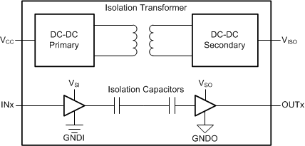
VCC is the
primary supply voltage referenced to GND1. VISO is the isolated supply voltage
referenced to GND2.
VSI and
VSO can be either VCC or VISO depending on the channel
direction.
VSI is the
input-side supply voltage referenced to GNDI and VSO is the output-side supply
voltage referenced to GNDO.
Simplified Schematic