SLPS732B june 2021 – april 2023 JFE150
PRODUCTION DATA
- 1 Features
- 2 Applications
- 3 Description
- 4 Revision History
- 5 Pin Configuration and Functions
- 6 Specifications
- 7 Parameter Measurement Information
- 8 Detailed Description
- 9 Application and Implementation
- 10Device and Documentation Support
- 11Mechanical, Packaging, and Orderable Information
Package Options
Mechanical Data (Package|Pins)
Thermal pad, mechanical data (Package|Pins)
Orderable Information
9.1.1 Input Protection Diodes
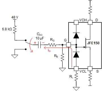
The JFE150 features diodes that are used to help clamp voltage surges that can occur on the input sensor to the gate. The diodes are connected between the gate and two separate pins, VCL and VCH. The clamping mechanism works by steering current from the gate into the VCL or VCH nodes when the voltage at the gate is less than VCL or greater than VCH. Figure 9-2 shows an example of a microphone input circuit where a dc blocking capacitor operates with a large dc voltage. When the microphone input is dropped or shorted, the dc blocking capacitor discharges into the VCL or VCH nodes, thus helping eliminate large signal transient voltages on the gate. There are also clamping diodes from the drain and source to VCL and VCH, respectively. The clamping diodes can withstand high surge currents up to 200 mA for 50 ms; however, limit dc current to less than 20 mA.
 Figure 9-1 JFE150 Clamping Diode
Example
Figure 9-1 JFE150 Clamping Diode
ExampleFigure 9-2 shows an example of configuring the diode clamp to protect the JFET against overvoltage in a phantom-powered microphone circuit. Phantom power typically delivers 48 V through a 6.8-kΩ pullup resistor to a microphone or dynamic load. If the microphone is disconnected, dc blocking capacitor CDC can be biased up to 48 V. If the input to the capacitor is then shorted to ground (shown by the switch in Figure 9-2), the gate voltage can exceed the absolute maximum rating for VGS. In this case, the blocking diode is used, along with current limiting resistors RG and RL, to clamp the gate voltage to a safe level. Be aware that the thermal noise of RG couples directly into the gate input; therefore, make sure to minimize the resistance of RG.
The clamping diodes are not required for operation. The VGS voltage can withstand –40 V, so clamping is not required if the VGS voltage is kept greater than this limit. If the diodes are not needed, leave the VCL and VCH nodes floating.
Most previous-generation JFET devices featured only three pins (gate, source, and drain). For these devices, the gate pin is in the same physical location as the VCL pin on the JFE150. To test the JFE150 in a three-pin socket, short pin 2 of the JFE150 (VCL) to pin 3 (G). When the devices are connected with pin 2 shorted to pin 3, the diode from VCL is shorted out and cannot provide any clamping protection. The input capacitance (CISS) also increases by 1 pF; see Figure 6-12.