SLIS183 June 2017 LM193-MIL
PRODUCTION DATA.
- 1 Features
- 2 Applications
- 3 Description
- 4 Revision History
- 5 Pin Configuration and Functions
- 6 Specifications
- 7 Detailed Description
- 8 Application and Implementation
- 9 Power Supply Recommendations
- 10Layout
- 11Device and Documentation Support
- 12Mechanical, Packaging, and Orderable Information
Package Options
Mechanical Data (Package|Pins)
Thermal pad, mechanical data (Package|Pins)
Orderable Information
7 Detailed Description
7.1 Overview
The dual comparator has the ability to operate up to absolute maximum of 36 V on the supply pin. This device has proven ubiquity and versatility across a wide range of applications. This is due to very wide supply voltages range (2 V to 36 V), low Iq and fast response of the device.
The open-drain output allows the user to configure the output's logic high voltage (VOH) and can be used to enable the comparator to be used in AND functionality.
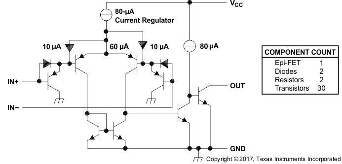
7.2 Functional Block Diagram
 Figure 6. Schematic (Each Comparator)
7.3 Feature Description
The comparator consists of a PNP darlington pair input, allowing the device to operate with very high gain and fast response with minimal input bias current. The input Darlington pair creates a limit on the input common mode voltage capability, allowing the comparator to accurately function from ground to VCC– 1.5 V input. Allow for VCC– 2 V at cold temperature.
The output consists of an open drain NPN (pull-down or low side) transistor. The output NPN will sink current when the negative input voltage is higher than the positive input voltage and the offset voltage. The VOL is resistive and will scale with the output current. See Figure 3 for VOL values with respect to the output current.
7.4 Device Functional Modes
7.4.1 Voltage Comparison
The device operates solely as a voltage comparator, comparing the differential voltage between the positive and negative pins and outputting a logic low or high impedance (logic high with pullup) based on the input differential polarity.