SLIS183 June 2017 LM193-MIL
PRODUCTION DATA.
- 1 Features
- 2 Applications
- 3 Description
- 4 Revision History
- 5 Pin Configuration and Functions
- 6 Specifications
- 7 Detailed Description
- 8 Application and Implementation
- 9 Power Supply Recommendations
- 10Layout
- 11Device and Documentation Support
- 12Mechanical, Packaging, and Orderable Information
Package Options
Mechanical Data (Package|Pins)
Thermal pad, mechanical data (Package|Pins)
Orderable Information
10 Layout
10.1 Layout Guidelines
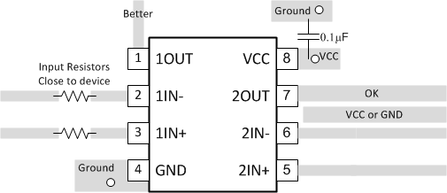
For accurate comparator applications without hysteresis it is important maintain a stable power supply with minimized noise and glitches. To achieve this, it is best to add a bypass capacitor between the supply voltage and ground. This should be implemented on the positive power supply and negative supply (if available). If a negative supply is not being used, do not put a capacitor between the device's GND pin and system ground.
Minimize coupling between outputs and inverting inputs to prevent output oscillations. Do not run output and inverting input traces in parallel unless there is a VCC or GND trace between output and inverting input traces to reduce coupling. When series resistance is added to inputs, place resistor close to the device.
10.2 Layout Example
 Figure 10. LM2903 Layout Example Used as an Example