SLCS005AG October 1979 – January 2025 LM193 , LM2903 , LM2903B , LM2903V , LM293 , LM293A , LM393 , LM393A , LM393B
PRODUCTION DATA
- 1
- 1 Features
- 2 Applications
- 3 Description
- 4 Pin Configuration and Functions
-
5 Specifications
- 5.1 Absolute Maximum Ratings
- 5.2 Recommended Operating Conditions
- 5.3 Thermal Information: LMx93x and LM2903x
- 5.4 ESD Ratings
- 5.5 Electrical Characteristics LM393B
- 5.6 Electrical Characteristics LM2903B
- 5.7 Switching Characteristics LM393B and LM2903B
- 5.8 Electrical Characteristics for LM193, LM293, and LM393 (without A suffix)
- 5.9 Electrical Characteristics for LM293A and LM393A
- 5.10 Electrical Characteristics for LM2903, LM2903V, and LM2903AV
- 5.11 Switching Characteristics: LM193, LM239, LM393, LM2903, all 'A' and 'V' versions
- 5.12 Typical Characteristics, LMx93x and LM2903x
- 6 Detailed Description
- 7 Application and Implementation
- 8 Device and Documentation Support
- 9 Revision History
- 10Mechanical, Packaging, and Orderable Information
Package Options
Mechanical Data (Package|Pins)
- D|8
Thermal pad, mechanical data (Package|Pins)
Orderable Information
4 Pin Configuration and Functions
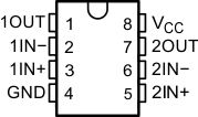
 Figure 4-1 D, DGK, JG, P, PS, DDF or PW Package8-Pin SOIC, VSSOP, PDIP, SO, or TSSOPTop View
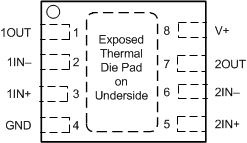
Connect thermal pad directly to GND pin.
Figure 4-2 DSG Package8-Pin WSON With Exposed PadTop ViewTable 4-1 Pin Functions
| PIN | I/O | DESCRIPTION | |||
|---|---|---|---|---|---|
| NAME | SOIC, VSSOP, PDIP, SO, DDF and TSSOP | DSG | |||
| 1OUT | 1 | 1 | Output | Output pin of comparator 1 | |
| 1IN– | 2 | 2 | Input | Negative input pin of comparator 1 | |
| 1IN+ | 3 | 3 | Input | Positive input pin of comparator 1 | |
| GND | 4 | 4 | — | Ground | |
| 2IN+ | 5 | 5 | Input | Positive input pin of comparator 2 | |
| 2IN- | 6 | 6 | Input | Negative input pin of comparator 2 | |
| 2OUT | 7 | 7 | Output | Output pin of comparator 2 | |
| VCC | 8 | 8 | — | Positive Supply | |
| Thermal Pad | — | PAD | — | Connect directly to GND pin | |