SNVS609K December 2008 – June 2022 LM25088 , LM25088-Q1
PRODUCTION DATA
- 1 Features
- 2 Applications
- 3 Description
- 4 Revision History
- 5 Pin Configuration and Functions
- 6 Specifications
-
7 Detailed Description
- 7.1 Overview
- 7.2 Functional Block Diagram
- 7.3
Feature Description
- 7.3.1 High Voltage Low-Dropout Regulator
- 7.3.2 Line Undervoltage Detector
- 7.3.3 Oscillator and Sync Capability
- 7.3.4 Error Amplifier and PWM Comparator
- 7.3.5 Ramp Generator
- 7.3.6 Dropout Voltage Reduction
- 7.3.7 Frequency Dithering (LM25088-1 Only)
- 7.3.8 Cycle-by-Cycle Current Limit
- 7.3.9 Overload Protection Timer (LM25088-2 Only)
- 7.3.10 Soft Start
- 7.3.11 HG Output
- 7.3.12 Thermal Protection
- 7.4 Device Functional Modes
-
8 Application and Implementation
- 8.1 Application Information
- 8.2
Typical Application
- 8.2.1 Design Requirements
- 8.2.2
Detailed Design Procedure
- 8.2.2.1 Timing Resistor
- 8.2.2.2 Output Inductor
- 8.2.2.3 Current Sense Resistor
- 8.2.2.4 Ramp Capacitor
- 8.2.2.5 Output Capacitors
- 8.2.2.6 Input Capacitors
- 8.2.2.7 VCC Capacitor
- 8.2.2.8 Bootstrap Capacitor
- 8.2.2.9 Soft-Start Capacitor
- 8.2.2.10 Output Voltage Divider
- 8.2.2.11 UVLO Divider
- 8.2.2.12 Restart Capacitor (LM5008-2 Only)
- 8.2.2.13 MOSFET Selection
- 8.2.2.14 Diode Selection
- 8.2.2.15 Snubber Components Selection
- 8.2.2.16 Error Amplifier Compensation
- 8.2.3 Application Curves
- 9 Power Supply Recommendations
- 10Layout
- 11Device and Documentation Support
- 12Mechanical, Packaging, and Orderable Information
Package Options
Mechanical Data (Package|Pins)
- PWP|16
Thermal pad, mechanical data (Package|Pins)
- PWP|16
Orderable Information
3 Description
The LM25088 high voltage non-synchronous buck controller features all the necessary functions to implement an efficient, high-voltage buck converter using the minimum number of external components. The LM25088 can be configured to operate over an ultra-wide input voltage range of 4.5 V to 42 V. This easy-to-use controller includes a level-shifted gate driver capable of controlling an external N-channel buck switch. The control method is based on peak current mode control utilizing an emulated current ramp. The use of an emulated control ramp reduces noise sensitivity of the pulse-width modulation circuit, allowing reliable control of very small duty cycles necessary in high input voltage and low output voltage applications. The LM25088 switching frequency is programmable from 50 kHz to 1 MHz.
The LM25088 is available in two versions: The LM25088-1 provides a ±5% frequency dithering function to reduce the conducted and radiated EMI while the LM25088-2 provides a versatile restart timer for overload protection. Additional features include a low dropout bias regulator, tri-level enable input to control shutdown and standby modes, soft start, and oscillator synchronization capability. The device is available in a thermally enhanced HTSSOP-16 pin package.
| Part Number | Package(1) | Body Size (NOM) |
|---|---|---|
| LM25088 | HTSSOP (16) | 5.00 mm × 4.40 mm |
| LM25088-Q1 |
 Simplified Schematic
 Typical Application Circuit
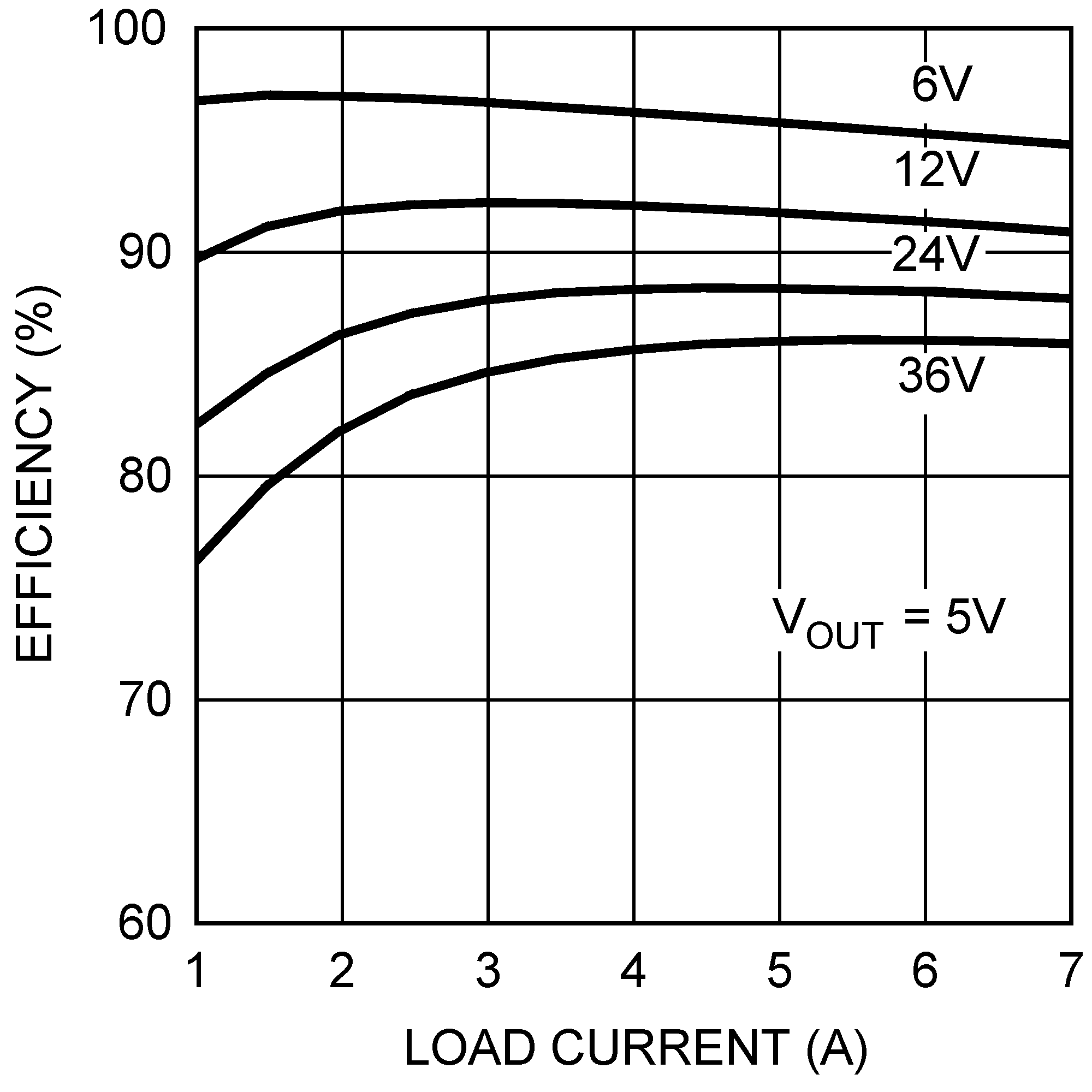
Efficiency