SNVSCT9 October 2024 LM251772
PRODUCTION DATA
- 1
- 1 Features
- 2 Applications
- 3 Description
- 4 Device Comparison
- 5 Pin Configuration and Functions
- 6 Specifications
- 7 Parameter Measurement Information
-
8 Detailed Description
- 8.1 Overview
- 8.2 Functional Block Diagram
- 8.3
Feature Description
- 8.3.1 Buck-Boost Control Scheme
- 8.3.2 Power Save Mode
- 8.3.3 Reference System
- 8.3.4 Supply Voltage Selection – VSMART Switch and Selection Logic
- 8.3.5 Enable and Undervoltage Lockout
- 8.3.6 Internal VCC Regulators
- 8.3.7 Error Amplifier and Control
- 8.3.8 Output Voltage Discharge
- 8.3.9 Peak Current Sensor
- 8.3.10 Short Circuit - Hiccup Protection
- 8.3.11 Current Monitor/Limiter
- 8.3.12 Oscillator Frequency Selection
- 8.3.13 Frequency Synchronization
- 8.3.14 Output Voltage Tracking
- 8.3.15 Slope Compensation
- 8.3.16 Configurable Soft Start
- 8.3.17 Drive Pin
- 8.3.18 Dual Random Spread Spectrum – DRSS
- 8.3.19 Gate Driver
- 8.3.20 Cable Drop Compensation (CDC)
- 8.3.21 CFG-pin and R2D Interface
- 8.3.22 Advanced Monitoring Features
- 8.3.23
Protection Features
- 8.3.23.1 Thermal Shutdown (TSD)
- 8.3.23.2 Over Current Protection
- 8.3.23.3 Output Over Voltage Protection 1 (OVP1)
- 8.3.23.4 Output Over Voltage Protection 2 (OVP2)
- 8.3.23.5 Input Voltage Protection (IVP)
- 8.3.23.6 Input Voltage Regulation (IVR)
- 8.3.23.7 Power Good
- 8.3.23.8 Boot-Strap Under Voltage Protection
- 8.3.23.9 Boot-strap Over Voltage Clamp
- 8.3.23.10 CRC - CHECK
- 8.4 Device Functional Modes
- 8.5 Programming
- 9 LM251772 Registers
-
10Application and Implementation
- 10.1 Application Information
- 10.2
Typical Application
- 10.2.1 Design Requirements
- 10.2.2
Detailed Design Procedure
- 10.2.2.1 Custom Design with WEBENCH Tools
- 10.2.2.2 Frequency
- 10.2.2.3 Feedback Divider
- 10.2.2.4 Inductor and Current Sense Resistor Selection
- 10.2.2.5 Output Capacitor
- 10.2.2.6 Input Capacitor
- 10.2.2.7 Slope Compensation
- 10.2.2.8 UVLO Divider
- 10.2.2.9 Soft-Start Capacitor
- 10.2.2.10 MOSFETs QH1 and QL1
- 10.2.2.11 MOSFETs QH2 and QL2
- 10.2.2.12 Loop Compensation
- 10.2.2.13 External Component Selection
- 10.2.3 Application Curves
- 10.3 Wireless Charging Supply
- 10.4 USB-PD Source with Power Path
- 10.5 Parallel (Multiphase) Operation
- 11Device and Documentation Support
- 12Revision History
- 13Mechanical, Packaging, and Orderable Information
Package Options
Mechanical Data (Package|Pins)
- RHA|40
Thermal pad, mechanical data (Package|Pins)
- RHA|40
Orderable Information
8.3.18 Dual Random Spread Spectrum – DRSS
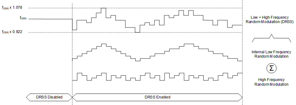
The device provides a digital spread spectrum, which reduces the EMI of the power supply over a wide frequency range. This function is selected by the R2D interface (Table 8-7) or the Register Table 9-10 . When the spread spectrum is enabled, the internal modulator dithers the internal clock. When an external synchronization clock is applied to the SYNC pin, the internal spread spectrum is disabled. DRSS combines a low frequency triangular modulation profile with a high frequency random modulation profile. The low frequency triangular modulation improves performance in lower radio frequency bands (for example, AM band), while the high frequency random modulation improves performance in higher radio frequency bands (for example, FM band). In addition, the frequency of the triangular modulation is further modulated randomly to reduce the likelihood of any audible tones. To minimize output voltage ripple caused by spread spectrum, duty cycle is modified on a cycle-by-cycle basis to maintain a nearly constant duty cycle when dithering is enabled.

Figure 8-28 Dual Random Spread Spectrum