SNVS457D February 2007 – October 2015 LM26400Y
PRODUCTION DATA.
- 1 Features
- 2 Applications
- 3 Description
- 4 Revision History
- 5 Pin Configuration and Functions
- 6 Specifications
- 7 Detailed Description
- 8 Application and Implementation
- 9 Power Supply Recommendations
- 10Layout
- 11Device and Documentation Support
- 12Mechanical, Packaging, and Orderable Information
Package Options
Mechanical Data (Package|Pins)
Thermal pad, mechanical data (Package|Pins)
- PWP|16
Orderable Information
9 Power Supply Recommendations
9.1 Low Input Voltage Considerations
When VIN is from 3 V to 5 V, TI recommends that an external bootstrap bias voltage and a Schottky diode be used to handle load currents up to 2 A. See Figure 32 for an illustration.
 Figure 32. External Bootstrap for Low VIN
The recommended voltage for the external bias is 5 V. Due to the absolute maximum rating of VBST - VSW, the external 5-V bias should not be higher than 6 V.
9.2 Programming Output Voltage
First make sure the required maximum duty cycle in steady state is less than 80% so that the regulator will not lose regulation. The datasheet lower limit for maximum duty cycle is about 90% over temperature (see Electrical Characteristics for the accurate value). The maximum duty cycle in steady state happens at low line and full load.
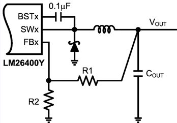
The output voltage is programmed through the feedback resistors R1 and R2, as illustrated in Figure 33.
 Figure 33. Programming Output Voltage
TI recommends that the lower feedback resistor R2 always be 5.9 kΩ. This simplifies the selection of the CFF value (for an explanation of CFF, see Load Step Response). The 5.9 kΩ is also a suitable R2 value in applications that need to increase the output voltage on the fly by paralleling another resistor with R2. Because the FB pin is 0.6 V during normal operation, the current through the feedback resistors is normally 0.6 V / 5.9 kΩ = 0.1 mA and the power dissipation in R2 is 0.6 V × 0.6 V / 5.9 kΩ = 61 µW - low enough for 0402 size or smaller resistors.
Use Equation 6 to determine the upper feedback resistor R1.

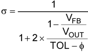
To determine the maximum allowed resistor tolerance, use Equation 7:

where
- TOL is the set point accuracy of the regulator
- Φ is the tolerance of VFB
Example:
VOUT = 1.2 V, with a set-point accuracy of ±3.5%.

Choose 1% resistors. R2 = 5.90 kΩ.
