SNVS543N January 2008 – June 2017 LM26480
PRODUCTION DATA.
- 1 Features
- 2 Applications
- 3 Description
- 4 Revision History
- 5 Device Options
- 6 Pin Configuration and Functions
-
7 Specifications
- 7.1 Absolute Maximum Ratings
- 7.2 ESD Ratings
- 7.3 Recommended Operating Conditions: Bucks
- 7.4 Thermal Information
- 7.5 General Electrical Characteristics
- 7.6 Low Dropout Regulators, LDO1 and LDO2
- 7.7 Buck Converters SW1, SW2
- 7.8 I/O Electrical Characteristics
- 7.9 Power On Reset Threshold/Function (POR)
- 7.10 Typical Characteristics — LDO
- 7.11 Typical Characteristics — Buck 2.8 V to 5.5 V
- 7.12 Typical Characteristics — Bucks 1 and 2
- 7.13 Typical Characteristics — Buck 3.6 V
-
8 Detailed Description
- 8.1 Overview
- 8.2 Functional Block Diagram
- 8.3
Feature Description
- 8.3.1
DC-DC Converters
- 8.3.1.1 Linear Low Dropout Regulators (LDOs)
- 8.3.1.2
SW1, SW2: Synchronous Step-Down Magnetic DC-DC Converters
- 8.3.1.2.1 Functional Description
- 8.3.1.2.2 Circuit Operation Description
- 8.3.1.2.3 Sync Function
- 8.3.1.2.4 PWM Operation
- 8.3.1.2.5 Internal Synchronous Rectification
- 8.3.1.2.6 Current Limiting
- 8.3.1.2.7 PFM Operation
- 8.3.1.2.8 SW1, SW2 Control
- 8.3.1.2.9 Shutdown Mode
- 8.3.1.2.10 Soft Start
- 8.3.1.2.11 Low Dropout Operation
- 8.3.1.2.12 Flexible Power-On Reset (Power Good with Delay)
- 8.3.1.2.13 Undervoltage Lockout
- 8.3.1
DC-DC Converters
- 8.4 Device Functional Modes
-
9 Application and Implementation
- 9.1 Application Information
- 9.2 Typical Application
- 10Power Supply Recommendations
- 11Layout
- 12Device and Documentation Support
- 13Mechanical, Packaging, and Orderable Information
Package Options
Mechanical Data (Package|Pins)
- RTW|24
Thermal pad, mechanical data (Package|Pins)
- RTW|24
Orderable Information
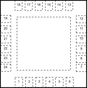
6 Pin Configuration and Functions
RTW Package
24-Pin WQFN
Top View

Pin Functions
| PIN | I/O | TYPE(1) | DESCRIPTION | |
|---|---|---|---|---|
| NO. | NAME | |||
| 1 | VINLDO12 | I | P | Analog power for internal functions (VREF, BIAS, I2C, Logic) |
| 2 | SYNC | I | G/(D) | Frequency synchronization pin, which allows the user to connect an external clock signal to synchronize the PMIC internal oscillator. Default OFF and must be grounded when not used. Part number LM26480SQ-BF has this feature enabled. Contact Texas Instruments Sales Office/Distributors for availability of LM26480SQ-BF. |
| 3 | NPOR | O | D | nPOR Power on reset pin for both Buck1 and Buck 2. Open drain logic output 100-kΩ pullup resistor. nPOR is pulled to ground when the voltages on these supplies are not good. See Flexible Power-On Reset (Power Good with Delay) for more information. |
| 4 | GND_SW1 | G | G | Buck1 NMOS power ground |
| 5 | SW1 | O | P | Buck1 switcher output pin |
| 6 | VIN1 | I | P | Power in from either DC source or battery to Buck1 |
| 7 | ENSW1 | I | D | Enable pin for Buck1 switcher, a logic HIGH enables Buck1. Pin cannot be left floating. |
| 8 | FB1 | I | A | Buck1 input feedback terminal |
| 9 | GND_C | G | G | Non-switching core ground pin |
| 10 | AVDD | I | P | Analog Power for Buck converters |
| 11 | FB2 | I | A | Buck2 input feedback terminal |
| 12 | ENSW2 | I | D | Enable pin for Buck2 switcher, a logic HIGH enables Buck2. Pin cannot be left floating. |
| 13 | VIN2 | I | P | Power in from either DC source or Battery to Buck2 |
| 14 | SW2 | O | P | Buck2 switcher output pin |
| 15 | GND_SW2 | G | G | Buck2 NMOS |
| 16 | ENLDO2 | I | D | LDO2 enable pin, a logic HIGH enables LDO2. Pin cannot be left floating. |
| 17 | ENLDO1 | I | D | LDO1 enable pin, a logic HIGH enables LDO1. Pin cannot be left floating. |
| 18 | GND_L | G | G | LDO ground |
| 19 | VINLDO1 | I | P | Power in from either DC source or battery to LDO1 |
| 20 | LDO1 | O | P | LDO1 Output |
| 21 | FBL1 | I | A | LDO1 feedback terminal |
| 22 | FBL2 | I | A | LDO2 feedback terminal |
| 23 | LDO2 | O | P | LDO output |
| 24 | VINLDO2 | I | P | Power in from either DC source or battery to LDO2. |
| DAP | DAP | G | G | Connection is not necessary for electrical performance, but it is recommended for better thermal dissipation. |
(1) A: Analog Pin, G: Ground Pin, P: Power Pin, I: Input Pin, O: Output Pin, D: Digital.