LM266x Switched Capacitor Voltage Converter
1 Features
- Inverts or Doubles Input Supply Voltage
- 3.5-Ω Typical Output Resistance
- 86% Typical Conversion Efficiency at 200 mA
- (LM2662) Selectable Oscillator Frequency: 20 kHz/150 kHz
- (LM2663) Low Current Shutdown Mode
2 Applications
- Laptop Computers
- Cellular Phones
- Medical Instruments
- Operational Amplifier Power Supplies
- Interface Power Supplies
- Handheld Instruments
Voltage Inverter

3 Description
The LM2662/LM2663 CMOS charge-pump voltage converter inverts a positive voltage in the range of 1.5 V to 5.5 V to the corresponding negative voltage. The LM2662/LM2663 uses two low cost capacitors to provide 200 mA of output current without the cost, size, and EMI related to inductor based converters. With an operating current of only 300 μA and operating efficiency greater than 90% at most loads, the LM2662/LM2663 provides ideal performance for battery powered systems. The LM2662/LM2663 may also be used as a positive voltage doubler.
The oscillator frequency can be lowered by adding an external capacitor to the OSC pin. Also, the OSC pin may be used to drive the LM2662/LM2663 with an external clock. For LM2662, a frequency control (FC) pin selects the oscillator frequency of 20 kHz or 150 kHz. For LM2663, an external shutdown (SD) pin replaces the FC pin. The SD pin can be used to disable the device and reduce the quiescent current to 10 μA. The oscillator frequency for LM2663 is 150 kHz.
Device Information(1)
| PART NUMBER | PACKAGE | BODY SIZE (NOM) |
|---|---|---|
| LM2662 | SOIC (8) | 4.90 mm x 3.91 mm |
| LM2663 |
- For all available packages, see the orderable addendum at the end of the datasheet.
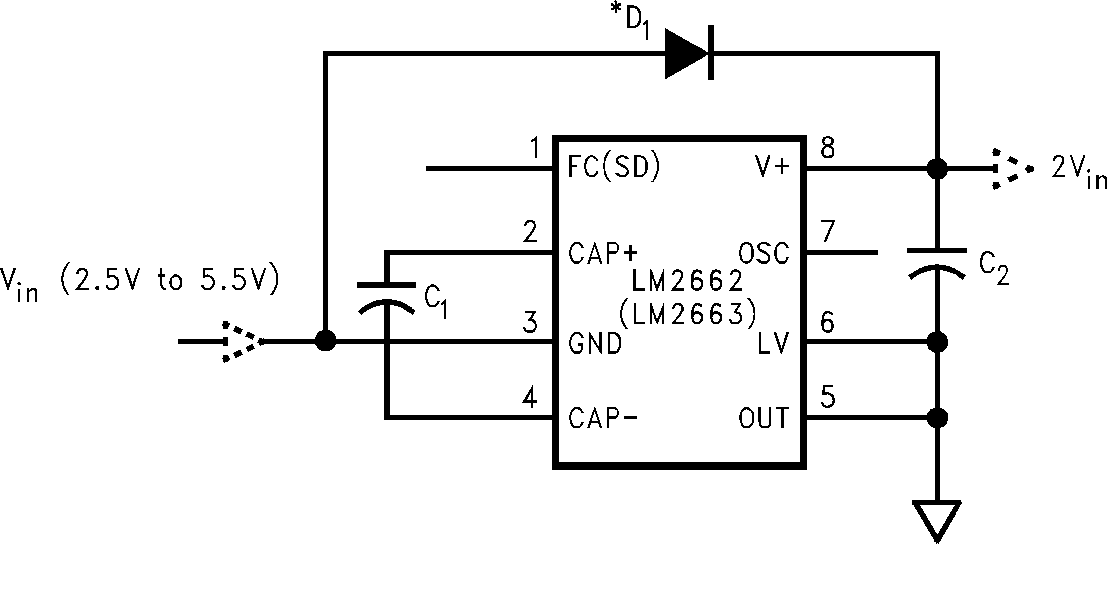
Splitting VIN in Half

4 Revision History
Changes from D Revision (May 2013) to E Revision
- Added Device Information and Handling Rating tables, Feature Description, Device Functional Modes, Application and Implementation, Power Supply Recommendations, Layout, Device and Documentation Support, and Mechanical, Packaging, and Orderable Information sections; moved some curves to Application Curves sectionGo
Changes from C Revision (May 2013) to D Revision
- Changed layout of National Data Sheet to TI formatGo
5 Pin Configuration and Functions
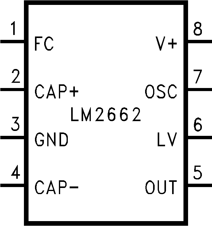
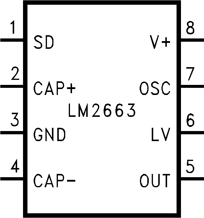
Pin Functions
| PIN | TYPE | DESCRIPTION | ||
|---|---|---|---|---|
| NUMBER | NAME | VOLTAGE INVERTER | VOLTAGE DOUBLER | |
| 1 | FC | Frequency control for internal oscillator: | Same as inverter. | |
| (LM2662) | Input | FC = open, ƒOSC = 20 kHz (typ); | ||
| FC = V+, ƒOSC = 150 kHz (typ); | ||||
| FC has no effect when OSC pin is driven externally. | ||||
| 1 | SD (LM2663) |
Input | Shutdown control pin, tie this pin to the ground in normal operation. | Same as inverter. |
| 2 | CAP+ | Power | Connect this pin to the positive terminal of charge-pump capacitor. | Same as inverter. |
| 3 | GND | Ground | Power supply ground input. | Power supply positive voltage input. |
| 4 | CAP− | Power | Connect this pin to the negative terminal of charge-pump capacitor. | Same as inverter. |
| 5 | OUT | Power | Negative voltage output. | Power supply ground input. |
| 6 | LV | Input | Low-voltage operation input. Tie LV to GND when input voltage is less than 3.5 V. Above 3.5 V, LV can be connected to GND or left open. When driving OSC with an external clock, LV must be connected to GND. | LV must be tied to OUT. |
| 7 | OSC | Input | Oscillator control input. OSC is connected to an internal 15-pF capacitor. An external capacitor can be connected to slow the oscillator. Also, an external clock can be used to drive OSC. | Same as inverter except that OSC cannot be driven by an external clock. |
| 8 | V+ | Power Input | Power supply positive voltage input. | Positive voltage output. |