SNVS002E January 1999 – October 2014 LM2662 , LM2663
PRODUCTION DATA.
- 1 Features
- 2 Applications
- 3 Description
- 4 Revision History
- 5 Pin Configuration and Functions
- 6 Specifications
- 7 Parameter Measurement Information
- 8 Detailed Description
- 9 Application and Implementation
- 10Power Supply Recommendations
- 11Layout
- 12Device and Documentation Support
- 13Mechanical, Packaging, and Orderable Information
Package Options
Mechanical Data (Package|Pins)
- D|8
Thermal pad, mechanical data (Package|Pins)
Orderable Information
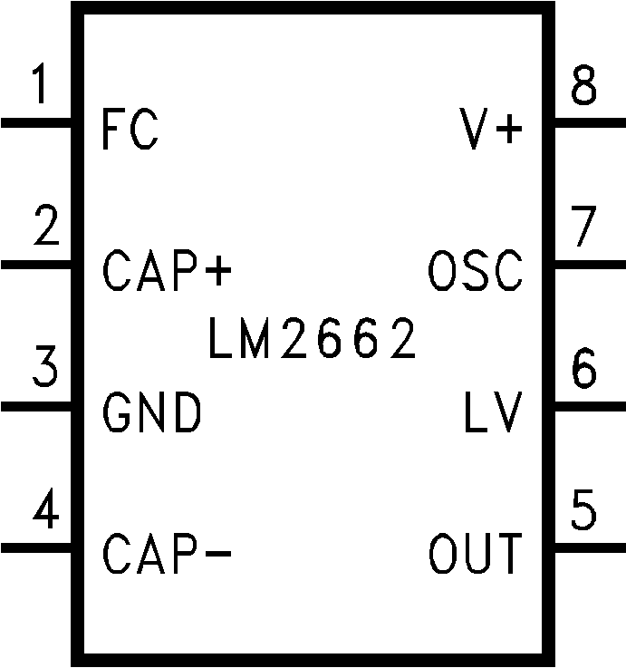
5 Pin Configuration and Functions
LM2662 SOIC (D)
8 Pins
Top View
LM2663 SOIC (D)
8 Pins
Top View
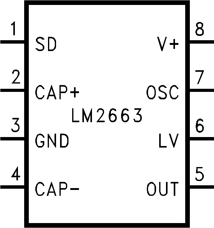
Pin Functions
| PIN | TYPE | DESCRIPTION | ||
|---|---|---|---|---|
| NUMBER | NAME | VOLTAGE INVERTER | VOLTAGE DOUBLER | |
| 1 | FC | Frequency control for internal oscillator: | Same as inverter. | |
| (LM2662) | Input | FC = open, ƒOSC = 20 kHz (typ); | ||
| FC = V+, ƒOSC = 150 kHz (typ); | ||||
| FC has no effect when OSC pin is driven externally. | ||||
| 1 | SD (LM2663) |
Input | Shutdown control pin, tie this pin to the ground in normal operation. | Same as inverter. |
| 2 | CAP+ | Power | Connect this pin to the positive terminal of charge-pump capacitor. | Same as inverter. |
| 3 | GND | Ground | Power supply ground input. | Power supply positive voltage input. |
| 4 | CAP− | Power | Connect this pin to the negative terminal of charge-pump capacitor. | Same as inverter. |
| 5 | OUT | Power | Negative voltage output. | Power supply ground input. |
| 6 | LV | Input | Low-voltage operation input. Tie LV to GND when input voltage is less than 3.5 V. Above 3.5 V, LV can be connected to GND or left open. When driving OSC with an external clock, LV must be connected to GND. | LV must be tied to OUT. |
| 7 | OSC | Input | Oscillator control input. OSC is connected to an internal 15-pF capacitor. An external capacitor can be connected to slow the oscillator. Also, an external clock can be used to drive OSC. | Same as inverter except that OSC cannot be driven by an external clock. |
| 8 | V+ | Power Input | Power supply positive voltage input. | Positive voltage output. |