SNVS180N April   2002  – April 2016 LM2750

PRODUCTION DATA.  

  1. Features
  2. Applications
  3. Description
  4. Revision History
  5. Pin Configuration and Functions
  6. Specifications
    1. 6.1 Absolute Maximum Ratings
    2. 6.2 ESD Ratings
    3. 6.3 Recommended Operating Conditions
    4. 6.4 Thermal Information
    5. 6.5 Electrical Characteristics
    6. 6.6 Switching Characteristics
    7. 6.7 Typical Characteristics
  7. Detailed Description
    1. 7.1 Overview
    2. 7.2 Functional Block Diagram
    3. 7.3 Feature Description
      1. 7.3.1 Pre-Regulation
      2. 7.3.2 Input, Output, and Ground Connections
      3. 7.3.3 Shutdown
      4. 7.3.4 Soft Start
      5. 7.3.5 Output Current Capability
      6. 7.3.6 Thermal Shutdown
      7. 7.3.7 Output Current Limiting
      8. 7.3.8 Programming the Output Voltage of the LM2750-ADJ
    4. 7.4 Device Functional Modes
      1. 7.4.1 PWM Brightness/Dimming Control
  8. Application and Implementation
    1. 8.1 Application Information
      1. 8.1.1 Output Voltage Ripple
    2. 8.2 Typical Applications
      1. 8.2.1 LM2750-ADJ Typical Application
        1. 8.2.1.1 Design Requirements
        2. 8.2.1.2 Detailed Design Procedure
          1. 8.2.1.2.1 Capacitors
          2. 8.2.1.2.2 Input Capacitor
          3. 8.2.1.2.3 Flying Capacitor
          4. 8.2.1.2.4 Output Capacitor
          5. 8.2.1.2.5 Power Efficiency And Power Dissipation
        3. 8.2.1.3 Application Curve
      2. 8.2.2 LM2750 LED Drive Applications
        1. 8.2.2.1 Design Requirements
        2. 8.2.2.2 Detailed Design Requirements
          1. 8.2.2.2.1 LED Driver Power Efficiency
        3. 8.2.2.3 Application Curve
  9. Power Supply Recommendations
    1. 9.1 LED Driver Power Consumption
  10. 10Layout
    1. 10.1 Layout Recommendations
    2. 10.2 Layout Example
  11. 11Device and Documentation Support
    1. 11.1 Device Support
      1. 11.1.1 Third-Party Products Disclaimer
    2. 11.2 Documentation Support
      1. 11.2.1 Related Documentation
      2. 11.2.2 Related Links
    3. 11.3 Community Resources
    4. 11.4 Trademarks
    5. 11.5 Electrostatic Discharge Caution
    6. 11.6 Glossary
  12. 12Mechanical, Packaging, and Orderable Information

Package Options

Mechanical Data (Package|Pins)
Thermal pad, mechanical data (Package|Pins)
Orderable Information

5 Pin Configuration and Functions

NGY or DSC Package
10-Pin WSON
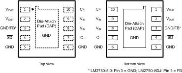
LM2750 LM2750-ADJ 20035102.gif
Pin Names and Numbers apply to both NGY0010A and DSC0010A packages.

Pin Functions

PIN TYPE DESCRIPTION
NAME LM2750-5.0 LM2750-ADJ
CAP+ 10 10 P Flying capacitor positive terminal
CAP– 7 7 P Flying capacitor negative terminal
FB 3 P Feedback pin
GND 3 G This pin must be connected externally to the ground pins (pins 5, 6, and the DAP).
GND 5, 6 5, 6 G Ground - These pins must be connected externally.
SD 4 4 I/O Active-low shutdown input. A 200-kΩ resistor is connected internally between this pin and GND to pull the voltage on this pin to 0 V, and shut the part down, when the pin is left floating.
VIN 8, 9 8, 9 P Input voltage - The pins must be connected externally.
VOUT 1, 2 1, 2 P Output voltage - These pins must be connected externally.
DAP GND The DAP (Exposed Pad) functions as a thermal connection when soldered to a copper plane.