SLCS141M May 2003 – December 2024 LM2903-Q1 , LM2903B-Q1
PRODUCTION DATA
- 1
- Features
- Applications
- Description
- 1Pin Configuration and Functions
-
2Specifications
- 2.1 Absolute Maximum Ratings, LM2903-Q1 and LM2903E-Q1
- 2.2 Absolute Maximum Ratings, LM2903B-Q1
- 2.3 ESD Ratings, LM2903-Q1 and LM2903E-Q1
- 2.4 ESD Ratings, LM2903B-Q1
- 2.5 Recommended Operating Conditions, LM2903B-Q1
- 2.6 Recommended Operating Conditions, LM2903-Q1
- 2.7 Recommended Operating Conditions, LM2903E-Q1
- 2.8 Thermal Information
- 2.9 Electrical Characteristics LM2903B - Q1
- 2.10 Switching Characteristics LM2903B - Q1
- 2.11 LM2903B-Q1 "T", "R" and "H" Temperature Test Options
- 2.12 Electrical Characteristics, LM2903-Q1 and LM2903E-Q1
- 2.13 Switching Characteristics, LM2903-Q1 and LM2903E-Q1
- 2.14 Typical Characteristics
- 3Detailed Description
- 4Application and Implementation
- 5Device and Documentation Support
- 6Revision History
- 7Mechanical, Packaging, and Orderable Information
Package Options
Refer to the PDF data sheet for device specific package drawings
Mechanical Data (Package|Pins)
- D|8
- DGK|8
- PW|8
Thermal pad, mechanical data (Package|Pins)
Orderable Information
1 Pin Configuration and Functions
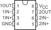
 Figure 1-1 D, DGK, DDF OR PW
PACKAGE
Figure 1-1 D, DGK, DDF OR PW
PACKAGETop View

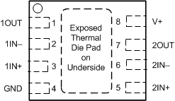
Connect thermal
pad directly to GND pin.
Figure 1-2 DSG
Package8-Pin WSON With Exposed Pad
Top View