SLCS005AG October 1979 – January 2025 LM193 , LM2903 , LM2903B , LM2903V , LM293 , LM293A , LM393 , LM393A , LM393B
PRODUCTION DATA
- 1
- 1 Features
- 2 Applications
- 3 Description
- 4 Pin Configuration and Functions
-
5 Specifications
- 5.1 Absolute Maximum Ratings
- 5.2 Recommended Operating Conditions
- 5.3 Thermal Information: LMx93x and LM2903x
- 5.4 ESD Ratings
- 5.5 Electrical Characteristics LM393B
- 5.6 Electrical Characteristics LM2903B
- 5.7 Switching Characteristics LM393B and LM2903B
- 5.8 Electrical Characteristics for LM193, LM293, and LM393 (without A suffix)
- 5.9 Electrical Characteristics for LM293A and LM393A
- 5.10 Electrical Characteristics for LM2903, LM2903V, and LM2903AV
- 5.11 Switching Characteristics: LM193, LM239, LM393, LM2903, all 'A' and 'V' versions
- 5.12 Typical Characteristics, LMx93x and LM2903x
- 6 Detailed Description
- 7 Application and Implementation
- 8 Device and Documentation Support
- 9 Revision History
- 10Mechanical, Packaging, and Orderable Information
Package Options
Mechanical Data (Package|Pins)
Thermal pad, mechanical data (Package|Pins)
- DSG|8
Orderable Information
7.2.3 Application Curves
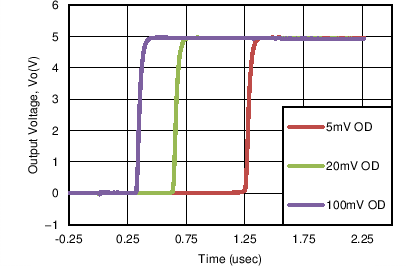
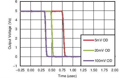
The following curves were generated with 5V on VCC and VLogic, RPULLUP = 5.1kΩ, and 50pF scope probe.
 Figure 7-2 Response Time for Various Overdrives (Positive Transition)
 Figure 7-3 Response Time for Various Overdrives (Negative Transition)