SNVSB33 May   2018 LM3102-Q1

PRODUCTION DATA.  

  1. Features
  2. Applications
  3. Description
    1.     Device Images
      1.      Typical Application Schematic
      2.      Efficiency vs Load Current (VOUT = 3.3 V)
  4. Revision History
  5. Pin Configuration and Functions
    1.     Pin Functions
  6. Specifications
    1. 6.1 Absolute Maximum Ratings
    2. 6.2 ESD Ratings
    3. 6.3 Recommended Operating Conditions
    4. 6.4 Thermal Information
    5. 6.5 Electrical Characteristics
    6. 6.6 Switching Characteristics
    7. 6.7 Typical Characteristics
  7. Detailed Description
    1. 7.1 Overview
    2. 7.2 Functional Block Diagram
    3. 7.3 Feature Description
      1. 7.3.1  COT Control Circuit Overview
      2. 7.3.2  Start-Up Regulator (VCC)
      3. 7.3.3  Regulation Comparator
      4. 7.3.4  Zero Coil Current Detect
      5. 7.3.5  Overvoltage Comparator
      6. 7.3.6  Current Limit
      7. 7.3.7  N-Channel MOSFET and Driver
      8. 7.3.8  Soft Start
      9. 7.3.9  Thermal Protection
      10. 7.3.10 Thermal Derating
    4. 7.4 Device Functional Modes
      1. 7.4.1 ON-Time Timer, Shutdown
  8. Application and Implementation
    1. 8.1 Application Information
    2. 8.2 Typical Application
      1. 8.2.1 Design Requirements
      2. 8.2.2 Detailed Design Procedure
        1. 8.2.2.1 Custom Design With WEBENCH® Tools
        2. 8.2.2.2 Design Steps for the LM3102-Q1 Application
        3. 8.2.2.3 External Components
      3. 8.2.3 Application Curve
    3. 8.3 System Examples
  9. Power Supply Recommendations
  10. 10Layout
    1. 10.1 Layout Guidelines
    2. 10.2 Layout Example
  11. 11Device and Documentation Support
    1. 11.1 Device Support
      1. 11.1.1 Development Support
        1. 11.1.1.1 Custom Design With WEBENCH® Tools
    2. 11.2 Receiving Notification of Documentation Updates
    3. 11.3 Community Resources
    4. 11.4 Trademarks
    5. 11.5 Electrostatic Discharge Caution
    6. 11.6 Glossary
  12. 12Mechanical, Packaging, and Orderable Information

Package Options

Mechanical Data (Package|Pins)
Thermal pad, mechanical data (Package|Pins)
Orderable Information

System Examples

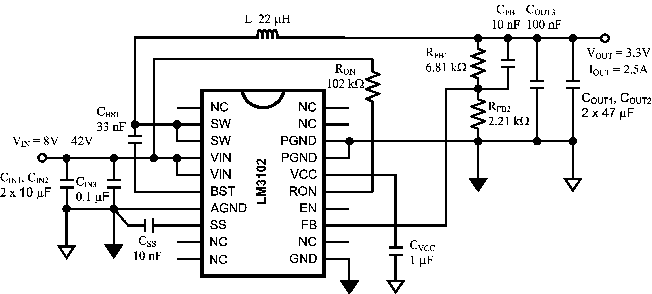
LM3102-Q1 30021335.pngFigure 28. Typical Application Schematic for VOUT = 3.3 V
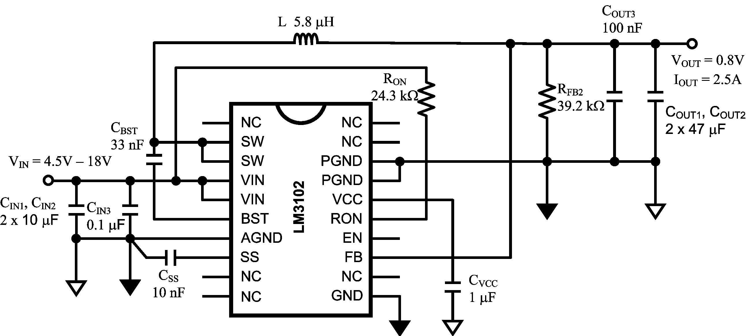
LM3102-Q1 30021336.pngFigure 29. Typical Application Schematic for VOUT = 0.8 V