SNVSB33 May   2018 LM3102-Q1

PRODUCTION DATA.  

  1. Features
  2. Applications
  3. Description
    1.     Device Images
      1.      Typical Application Schematic
      2.      Efficiency vs Load Current (VOUT = 3.3 V)
  4. Revision History
  5. Pin Configuration and Functions
    1.     Pin Functions
  6. Specifications
    1. 6.1 Absolute Maximum Ratings
    2. 6.2 ESD Ratings
    3. 6.3 Recommended Operating Conditions
    4. 6.4 Thermal Information
    5. 6.5 Electrical Characteristics
    6. 6.6 Switching Characteristics
    7. 6.7 Typical Characteristics
  7. Detailed Description
    1. 7.1 Overview
    2. 7.2 Functional Block Diagram
    3. 7.3 Feature Description
      1. 7.3.1  COT Control Circuit Overview
      2. 7.3.2  Start-Up Regulator (VCC)
      3. 7.3.3  Regulation Comparator
      4. 7.3.4  Zero Coil Current Detect
      5. 7.3.5  Overvoltage Comparator
      6. 7.3.6  Current Limit
      7. 7.3.7  N-Channel MOSFET and Driver
      8. 7.3.8  Soft Start
      9. 7.3.9  Thermal Protection
      10. 7.3.10 Thermal Derating
    4. 7.4 Device Functional Modes
      1. 7.4.1 ON-Time Timer, Shutdown
  8. Application and Implementation
    1. 8.1 Application Information
    2. 8.2 Typical Application
      1. 8.2.1 Design Requirements
      2. 8.2.2 Detailed Design Procedure
        1. 8.2.2.1 Custom Design With WEBENCH® Tools
        2. 8.2.2.2 Design Steps for the LM3102-Q1 Application
        3. 8.2.2.3 External Components
      3. 8.2.3 Application Curve
    3. 8.3 System Examples
  9. Power Supply Recommendations
  10. 10Layout
    1. 10.1 Layout Guidelines
    2. 10.2 Layout Example
  11. 11Device and Documentation Support
    1. 11.1 Device Support
      1. 11.1.1 Development Support
        1. 11.1.1.1 Custom Design With WEBENCH® Tools
    2. 11.2 Receiving Notification of Documentation Updates
    3. 11.3 Community Resources
    4. 11.4 Trademarks
    5. 11.5 Electrostatic Discharge Caution
    6. 11.6 Glossary
  12. 12Mechanical, Packaging, and Orderable Information

Package Options

Mechanical Data (Package|Pins)
Thermal pad, mechanical data (Package|Pins)
Orderable Information

Typical Characteristics

All curves are taken at VIN = 18 V with the configuration in the typical application circuit for VOUT = 3.3 V shown in this data sheet. TA = 25°C, unless otherwise specified.
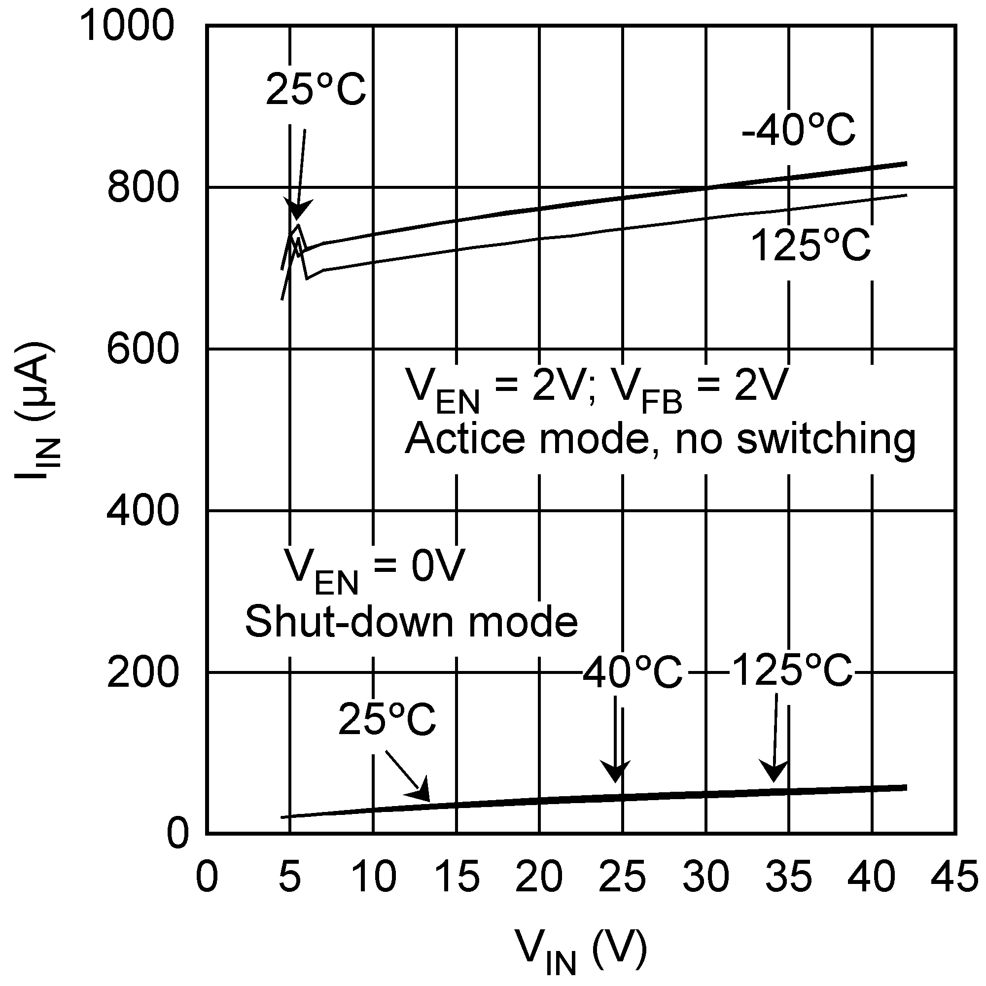
LM3102-Q1 30021303.png
Figure 1. Quiescent Current, IIN vs VIN
LM3102-Q1 30021305.png
Figure 3. VCC vs VIN
LM3102-Q1 30021307.png
Figure 5. Switching Frequency, fSW vs VIN
LM3102-Q1 30021309.png
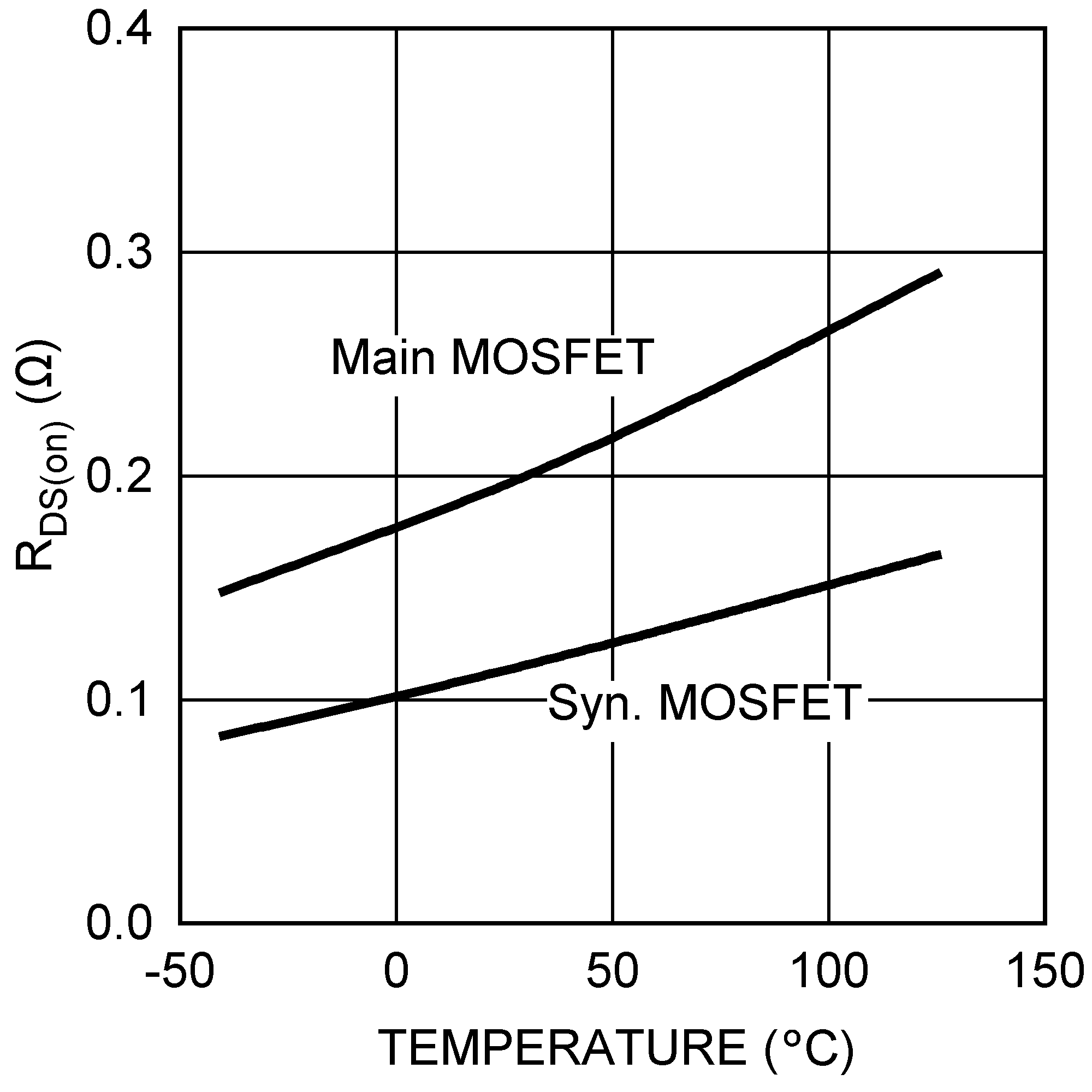
Figure 7. RDS(on) vs Temperature
LM3102-Q1 30021311.png
Figure 9. VOUT Regulation vs Load Current (VOUT = 3.3 V)
LM3102-Q1 30021313.png
Figure 11. VOUT Regulation vs Load Current (VOUT = 0.8 V)
LM3102-Q1 30021314.png
Figure 13. Enable Transient (VOUT = 3.3 V, 2.5 A Loaded)
LM3102-Q1 30021316.png
Figure 15. Continuous Mode Operation (VOUT = 3.3 V, 2.5 A Loaded)
LM3102-Q1 30021318.png
Figure 17. DCM to CCM Transition (VOUT = 3.3 V,
0.15-A - 2.5-A Load)
LM3102-Q1 30021304.png
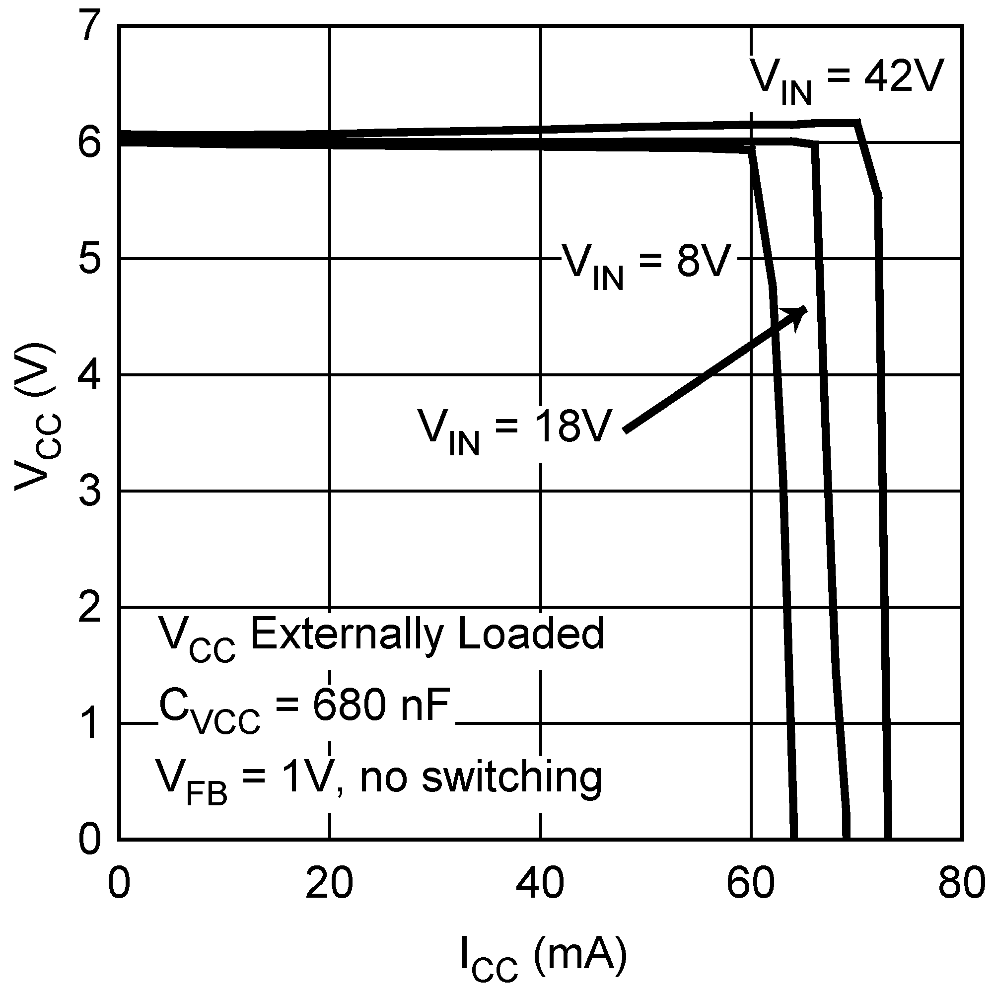
Figure 2. VCC vs ICC
LM3102-Q1 30021306.png
Figure 4. ton vs VIN
LM3102-Q1 30021308.png
Figure 6. VFB vs Temperature
LM3102-Q1 30021310.png
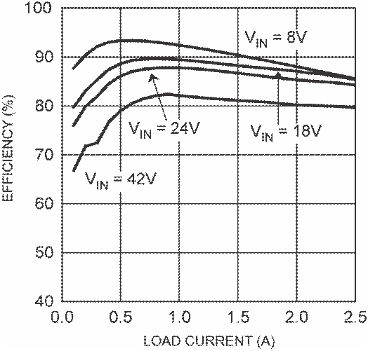
Figure 8. Efficiency vs Load Current (VOUT = 3.3 V)
LM3102-Q1 30021312.png
Figure 10. Efficiency vs Load Current (VOUT = 0.8 V)
LM3102-Q1 30021339.png
Figure 12. Power Up (VOUT = 3.3 V, 2.5 A Loaded)
LM3102-Q1 30021315.png
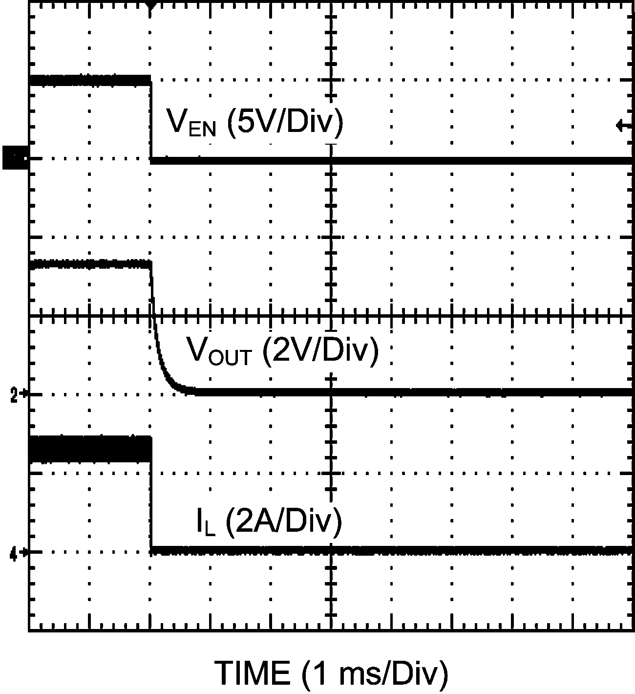
Figure 14. Shutdown Transient (VOUT = 3.3 V, 2.5 A Loaded)
LM3102-Q1 30021317.png
Figure 16. Discontinuous Mode Operation (VOUT = 3.3 V, 0.025 A Loaded)
LM3102-Q1 30021319.png
Figure 18. Load Transient (VOUT = 3.3 V, 0.25-A - 2.5-A Load, Current Slew Rate: 2.5 A/µs)