SNOSB48E October 2011 – August 2015 LM3242
PRODUCTION DATA.
- 1 Features
- 2 Applications
- 3 Description
- 4 Revision History
- 5 Pin Configuration and Functions
- 6 Specifications
- 7 Detailed Description
- 8 Application and Implementation
- 9 Power Supply Recommendations
- 10Layout
- 11Device and Documentation Support
- 12Mechanical, Packaging, and Orderable Information
Package Options
Mechanical Data (Package|Pins)
- YFQ|9
Thermal pad, mechanical data (Package|Pins)
Orderable Information
7 Detailed Description
7.1 Overview
The LM3242 is a simple, step-down DC-DC converter optimized for powering RF power amplifiers (PAs) in mobile phones, portable communicators, and similar battery-powered RF devices. It is designed to allow the RF PA to operate at maximum efficiency over a wide range of power levels from a single Li-Ion battery cell. It is based on a voltage-mode buck architecture, with synchronous rectification for high efficiency. The device is designed for a maximum load capability of 750 mA in PWM mode. Maximum load range may vary from this depending on input voltage, output voltage, and the inductor chosen.
There are five modes of operation depending on the current required: PWM (Pulse Width Modulation), ECO (ECOnomy), BP (Bypass), Sleep, and Shutdown. (See Table 1.) The LM3242 operates in PWM mode at higher load current conditions. Lighter loads cause the device to automatically switch into ECO mode. Shutdown mode turns the device off and reduces battery consumption to 0.1 µA (typical).
DC PWM mode output voltage precision is ±2% for 3.6 VOUT. Efficiency is typically around 95% (typical) for a 500-mA load with 3.3-V output, 3.9-V input. The output voltage is dynamically programmable from 0.4 V to 3.6 V by adjusting the voltage on the control pin (VCON) without the need for external feedback resistors. This ensures longer battery life by being able to change the PA supply voltage dynamically depending on its transmitting power.
Additional features include current overload protection and thermal overload shutdown.
The LM3242 is constructed using a chip-scale 9-bump DSBGA package. This package offers the smallest possible size, for space-critical applications such as cell phones, where board area is an important design consideration. Use of a high switching frequency (6 MHz, typical) reduces the size of external components. As shown in the Typical Application Circuit, only three external power components are required for implementation. Use of a DSBGA package requires special design considerations for implementation. (See DSBGA Package Assembly and Use.) Its fine bump-pitch requires careful board design and precision assembly equipment. Use of this package is best suited for opaque-case applications, where its edges are not subject to high-intensity ambient red or infrared light. Also, the system controller must set EN low during power-up and other low supply voltage conditions. (See Shutdown Mode.)
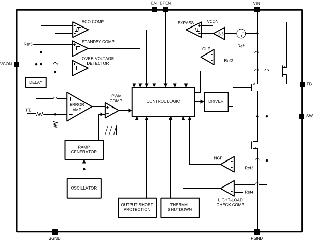
7.2 Functional Block Diagram

7.3 Feature Description
7.3.1 Circuit Operation
Referring to the Typical Application and Functional Block Diagram, the LM3242 operates as follows. During the first part of each switching cycle, the control block in the LM3242 turns on the internal top-side PFET switch. This allows current to flow from the input through the inductor to the output filter capacitor and load. The inductor limits the current to a ramp with a slope of around (VIN− VOUT) / L, by storing energy in a magnetic field. During the second part of each cycle, the controller turns the PFET switch off, blocking current flow from the input, and then turns the bottom-side NFET synchronous rectifier on. In response, the inductor’s magnetic field collapses, generating a voltage that forces current from ground through the synchronous rectifier to the output filter capacitor and load. As the stored energy is transferred back into the circuit and depleted, the inductor current ramps down with a slope around VOUT / L. The output filter capacitor stores charge when the inductor current is high, and releases it when low, smoothing the voltage across the load.
The output voltage is regulated by modulating the PFET switch on time to control the average current sent to the load. The effect is identical to sending a duty-cycle modulated rectangular wave formed by the switch and synchronous rectifier at SW to a low-pass filter formed by the inductor and output filter capacitor. The output voltage is equal to the average voltage at the SW pin.
7.3.2 Internal Synchronous Rectification
While in PWM mode, the LM3242 uses an internal NFET as a synchronous rectifier to reduce rectifier forward voltage drop and associated power loss. Synchronous rectification provides a significant improvement in efficiency whenever the output voltage is relatively low compared to the voltage drop across an ordinary rectifier diode.
With medium and heavy loads, the NFET synchronous rectifier is turned on during the inductor current down slope in the second part of each cycle. The synchronous rectifier is turned off prior to the next cycle. The NFET is designed to conduct through its intrinsic body diode during transient intervals before it turns on, eliminating the need for an external diode.
7.3.3 Current Limiting
The current limit feature allows the LM3242 to protect itself and external components during overload conditions. In PWM mode, the cycle-by-cycle current limit is a 1450 mA (typical). If an excessive load pulls the output voltage down to less than 0.3V (typical), the NFET synchronous rectifier is disabled and the current limit is reduced to 530 mA (typical). Moreover, when the output voltage becomes less than 0.15V (typical), the switching frequency decreases to 3 MHz, thereby preventing excess current and thermal stress.
7.3.4 Dynamically Adjustable Output Voltage
The LM3242 features dynamically adjustable output voltage to eliminate the need for external feedback resistors. The output can be set from 0.4 V to 3.6 V by changing the voltage on the analog VCON pin. This feature is useful in PA applications where peak power is needed only when the handset is far away from the base station or when data is being transmitted. In other instances the transmitting power can be reduced. Hence the supply voltage to the PA can be reduced, promoting longer battery life. See Setting The Output Voltage in Application and Implementation for further details. The LM3242 moves into pulse-skipping mode when duty cycle is over approximately 92% or less than approximately 15% and the output voltage ripple increases slightly.
7.3.5 Thermal Overload Protection
The LM3242 has a thermal overload protection function that operates to protect itself from short-term misuse and overload conditions. When the junction temperature exceeds around 150°C, the device inhibits operation. Both the PFET and the NFET are turned off. When the temperature drops below 125°C, normal operation resumes. Prolonged operation in thermal overload conditions may damage the device and is considered bad practice.
7.3.6 Soft Start
The LM3242 has a soft-start circuit that limits in-rush current during start-up. During start-up the switch current limit is increased in steps. Soft start is activated if EN goes from low to high after VIN reaches 2.7V.
7.4 Device Functional Modes
Table 1. Description Of Modes
| MODE | EN | BPEN | VCON | IOUT |
|---|---|---|---|---|
| Shutdown | 0 | X | X | X |
| Sleep | 1 | 0 | < 80 mV | X |
| Pulse Width Modulation (PWM) | 1 | 0 | > 130 mV, < (VIN − 0.2 V)/2.5 | > 100 mA |
| Economy (ECO) | 1 | 0 | < 50 mA | |
| Bypass (BP) | 1 | 0 | > (VIN − 0.2 V)/2.5 | X |
| 1 | 1 | X | X |
7.4.1 PWM Mode Operation
While in PWM mode operation, the converter operates as a voltage-mode controller with input voltage feedforward. This allows the converter to achieve excellent load and line regulation. The DC gain of the power stage is proportional to the input voltage. To eliminate this dependence, feed forward inversely proportional to the input voltage is introduced. While in PWM mode, the output voltage is regulated by switching at a constant frequency and then modulating the energy per cycle to control power to the load. At the beginning of each clock cycle the PFET switch is turned on and the inductor current ramps up until the comparator trips and the control logic turns off the switch. The current limit comparator can also turn off the switch in case the current limit of the PFET is exceeded. Then the NFET switch is turned on and the inductor current ramps down. The next cycle is initiated by the clock turning off the NFET and turning on the PFET.
7.4.2 Bypass Mode Operation
The LM3242 contains an internal BPFET switch for bypassing the PWM DC-DC converter during Bypass mode. In Bypass mode, this BPFET is turned on to power the PA directly from the battery for maximum RF output power. When the part operates in the Bypass mode, the output voltage is the input voltage less the voltage drop across the resistance of the BPFET in parallel with the PFET + Switch Inductor. Bypass mode is more efficient than operating in PWM mode at 100% duty cycle because the combined resistance is significantly less than the series resistance of the PWM PFET and inductor. This translates into higher voltage available on the output in Bypass mode, for a given battery voltage. The part can be set to bypass mode by sending BPEN pin high. This is called Forced Bypass Mode and it remains in bypass mode until BPEN pin goes low. Alternatively the part can go into Bypass mode automatically. This is called Auto-Bypass mode or Automatic Bypass mode. The bypass switch turns on when the difference between the input voltage and programmed output voltage is less than 200 mV (typical) for longer than 10 µs (typical). The bypass switch turns off when the input voltage is higher than the programmed output voltage by 250 mV (typical) for longer than 0.1 µs (typical). This method is very system resource friendly in that the Bypass PFET is turned on automatically when the input voltage gets close to the output voltage, a typical scenario of a discharging battery. It is also turned off automatically when the input voltage rises, a typical scenario when connecting a charger. When VOUT < 300 mV, BPEN is ignored.
7.4.3 ECO Mode Operation
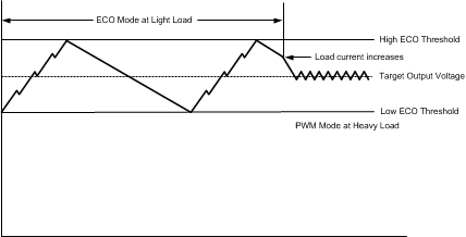
At very light loads (50 mA to 100 mA), the LM3242 enters ECO mode operation with reduced switching frequency and supply current to maintain high efficiency. During ECO mode operation, the LM3242 positions the output voltage slightly higher (7 mV typical) than the normal output voltage during PWM mode operation, allowing additional headroom for voltage drop during a load transient from light to heavy load.
 Figure 22. Operation In ECO Mode and Transfer to PWM Mode
7.4.4 Sleep Mode Operation
When VCON is less than 80 mV in 10 µs, the LM3242 goes into SLEEP mode — the SW pin is in Tri-state (floating), which operates like ECO mode with no switching. The LM3242 device returns to normal operation immediately when VCON ≥ 130 mV in PWM mode or ECO mode, depending on load detection.
7.4.5 Shutdown Mode
Setting the EN digital pin low (< 0.4 V) places the LM3242 in Shutdown mode (0.1 µA typical). During shutdown, the PFET switch, the NFET synchronous rectifier, reference voltage source, control and bias circuitry of the LM3242 are turned off. Setting EN high (> 1.2 V) enables normal operation. EN must be set low to turn off the LM3242 during power-up and undervoltage conditions when the power supply is less than the 2.7V minimum operating voltage. The LM3242 has an undervoltage lock-out (UVLO) comparator to turn the power device off in the case the input voltage or battery voltage is too low. The typical UVLO threshold is around 2 V for lock and 2.1 V for release.