SNVS465G October 2006 – September 2015 LM3404 , LM3404HV
PRODUCTION DATA.
- 1 Features
- 2 Applications
- 3 Description
- 4 Revision History
- 5 Pin Configuration and Functions
- 6 Specifications
- 7 Detailed Description
-
8 Application and Implementation
- 8.1 Application Information
- 8.2 Typical Applications
- 9 Power Supply Recommendations
- 10Layout
- 11Device and Documentation Support
- 12Mechanical, Packaging, and Orderable Information
Package Options
Mechanical Data (Package|Pins)
Thermal pad, mechanical data (Package|Pins)
Orderable Information
8 Application and Implementation
NOTE
Information in the following applications sections is not part of the TI component specification, and TI does not warrant its accuracy or completeness. TI’s customers are responsible for determining suitability of components for their purposes. Customers should validate and test their design implementation to confirm system functionality.
8.1 Application Information
8.1.1 Switching Frequency
Switching frequency is selected based on the trade-offs between efficiency (better at low frequency), solution size and cost (smaller at high frequency), and the range of output voltage that can be regulated (wider at lower frequency). Many applications place limits on switching frequency due to EMI sensitivity. The on-time of the LM3404 and LM3404HV devices can be programmed for switching frequencies ranging from the 10’s of kHz to over 1 MHz. The maximum switching frequency is limited only by the minimum on-time and minimum off-time requirements.
8.1.2 LED Ripple Current
Selection of the ripple current, ΔiF, through the LED array is analogous to the selection of output ripple voltage in a standard voltage regulator. Where the output ripple in a voltage regulator is commonly ±1% to ±5% of the DC output voltage, LED manufacturers generally recommend values for ΔiF ranging from ±5% to ±20% of IF. Higher LED ripple current allows the use of smaller inductors, smaller output capacitors, or no output capacitors at all. The advantages of higher ripple current are reduction in the solution size and cost. Lower ripple current requires more output inductance, higher switching frequency, or additional output capacitance. The advantages of lower ripple current are a reduction in heating in the LED itself and greater tolerance in the average LED current before the current limit of the LED or the driving circuitry is reached.
8.1.3 Buck Converters Without Output Capacitors
The buck converter is unique among non-isolated topologies because of the direct connection of the inductor to the load during the entire switching cycle. By definition an inductor will control the rate of change of current that flows through it, and this control overcurrent ripple forms the basis for component selection in both voltage regulators and current regulators. A current regulator such as the LED driver for which the LM3404 and LM3404HV devices was designed focuses on the control of the current through the load, not the voltage across it. A constant current regulator is free of load current transients, and has no need of output capacitance to supply the load and maintain output voltage. Referring to Typical Application Diagram on the front page of this data sheet, the inductor and LED can form a single series chain, sharing the same current. When no output capacitor is used, the same equations that govern inductor ripple current, ΔiL, also apply to the LED ripple current, ΔiF. For a controlled on-time converter such as the LM3404 and LM3404HV devices, the ripple current is described by Equation 9.

A minimum ripple voltage of 25 mV is recommended at the CS pin to provide good signal to noise ratio (SNR). The CS pin ripple voltage, ΔvSNS, is described by Equation 10.
8.1.4 Buck Converters With Output Capacitors
A capacitor placed in parallel with the LED or array of LEDs can be used to reduce the LED current ripple while keeping the same average current through both the inductor and the LED array. This technique is demonstrated in Design Examples 1 and 2. With this topology the output inductance can be lowered, making the magnetics smaller and less expensive. Alternatively, the circuit could be run at lower frequency but keep the same inductor value, improving the efficiency and expanding the range of output voltage that can be regulated. Both the peak current limit and the OVP/OCP comparator still monitor peak inductor current, placing a limit on how large ΔiL can be even if ΔiF is made very small. A parallel output capacitor is also useful in applications where the inductor or input voltage tolerance is poor. Adding a capacitor that reduces ΔiF to well below the target provides headroom for changes in inductance or VIN that might otherwise push the peak LED ripple current too high.
Figure 20 shows the equivalent impedances presented to the inductor current ripple when an output capacitor, CO, and its equivalent series resistance (ESR) are placed in parallel with the LED array. The entire inductor ripple current flows through RSNS to provide the required 25 mV of ripple voltage for proper operation of the CS comparator.
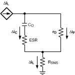 Figure 20. LED and CO Ripple Current
To calculate the respective ripple currents the LED array is represented as a dynamic resistance, rD. LED dynamic resistance is not always specified on the manufacturer’s data sheet, but it can be calculated as the inverse slope of the LED’s VF vs. IF curve. Dividing VF by IF will give an incorrect value that is 5× to 10× too high. Total dynamic resistance for a string of n LEDs connected in series can be calculated as the rD of one device multiplied by n. Inductor ripple current is still calculated with the expression from Buck Converters Without Output Capacitors. Equation 11 can then be used to estimate ΔiF when using a parallel capacitor.

The calculation for ZC assumes that the shape of the inductor ripple current is approximately sinusoidal.
Small values of CO that do not significantly reduce ΔiF can also be used to control EMI generated by the switching action of the LM3404 and LM3404HV devices. EMI reduction becomes more important as the length of the connections between the LED and the rest of the circuit increase.
8.1.5 Input Capacitors
Input capacitors at the VIN pin of the LM3404 and LM3404HV devices are selected using requirements for minimum capacitance and rms ripple current. The input capacitors supply pulses of current approximately equal to IF while the power MOSFET is on, and are charged up by the input voltage while the power MOSFET is off. Switching converters such as the LM3404 and LM3404HV devices have a negative input impedance due to the decrease in input current as input voltage increases. This inverse proportionality of input current to input voltage can cause oscillations (sometimes called power supply interaction) if the magnitude of the negative input impedance is greater the the input filter impedance. Minimum capacitance can be selected by comparing the input impedance to the converter’s negative resistance; however this requires accurate calculation of the input voltage source inductance and resistance, quantities that can be difficult to determine.
An alternative method to select the minimum input capacitance, CIN(MIN), is to select the maximum input voltage ripple which can be tolerated. This value, ΔvIN(MAX), is equal to the change in voltage across CIN during the converter on-time, when CIN supplies the load current. CIN(MIN) can be selected with Equation 12.

A good starting point for selection of CIN is to use an input voltage ripple of 5% to 10% of VIN. TI recommends a minimum input capacitance of 2× the CIN(MIN) value for all LM3404 and LM3404HV circuits. To determine the rms current rating, Equation 13 can be used.

Ceramic capacitors are the best choice for the input to the LM3404 and LM3404HV devices due to their high ripple current rating, low ESR, low cost, and small size compared to other types. When selecting a ceramic capacitor, special attention must be paid to the operating conditions of the application. Ceramic capacitors can lose one-half or more of their capacitance at their rated DC voltage bias and also lose capacitance with extremes in temperature. TI recommends a DC voltage rating equal to twice the expected maximum input voltage. In addition, the minimum quality dielectric which is suitable for switching power supply inputs is X5R, while X7R or better is preferred.
8.1.6 Recirculating Diode
The LM3404 and LM3404HV devices are non-synchronous buck regulators that require a recirculating diode D1 (see the Typical Application Diagram) to carrying the inductor current during the MOSFET off-time. The most efficient choice for D1 is a Schottky diode due to low forward drop and near-zero reverse recovery time. D1 must be rated to handle the maximum input voltage plus any switching node ringing when the MOSFET is on. In practice all switching converters have some ringing at the switching node due to the diode parasitic capacitance and the lead inductance. D1 must also be rated to handle the average current, ID, calculated as shown in Equation 14.
This calculation must be done at the maximum expected input voltage. The overall converter efficiency becomes more dependent on the selection of D1 at low duty cycles, where the recirculating diode carries the load current for an increasing percentage of the time. This power dissipation can be calculating by checking the typical diode forward voltage, VD, from the I-V curve on the product data sheet and then multiplying it by ID. Diode data sheets will also provide a typical junction-to-ambient thermal resistance, θJA, which can be used to estimate the operating die temperature of the device. Multiplying the power dissipation (PD = ID × VD) by θJA gives the temperature rise. The diode case size can then be selected to maintain the Schottky diode temperature below the operational maximum.
8.1.7 LED Current During DIM Mode
The LM3404 contains high speed MOSFET gate drive circuitry that switches the main internal power MOSFET between on and off states. This circuitry uses current derived from the VCC regulator to charge the MOSFET during turn-on, then dumps current from the MOSFET gate to the source (the SW pin) during turn-off. As shown in Figure 19, the MOSFET drive circuitry contains a gate drive undervoltage lockout (UVLO) circuit that ensures the MOSFET remains off when there is inadequate VCC voltage for proper operation of the driver. This watchdog circuitry is always running including during DIM and shutdown modes, and supplies a small amount of current from VCC to SW. Because the SW pin is connected directly to the LEDs through the buck inductor, this current returns to ground through the LEDs. The amount of current sourced is a function of the SW voltage, as shown in Figure 21.
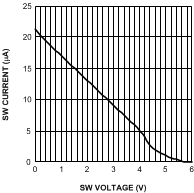 Figure 21. LED Current From SW Pin
Though most power LEDs are designed to run at several hundred milliamps, some can be seen to glow with a faint light at extremely low current levels, as low as a couple microamps in some instances. In lab testing, the forward voltage was found to be approximately 2 V for LEDs that exhibited visible light at these low current levels. For LEDs that did not show light emission at very low current levels, the forward voltage was found to be around 900 mV. It is important to remember that the forward voltage is also temperature dependent, decreasing at higher temperatures. Consequently, with a maximum Vcc voltage of 7.4 V, current will be observed in the LEDs if the total stack voltage is less than about 6 V at a forward current of several microamps. No current is observed if the stack voltage is above 6 V, as shown in Figure 21. The need for absolute darkness during DIM mode is also application dependent. It will not affect regular PWM dimming operation.
The fix for this issue is extremely simple. Place a resistor from the SW pin to ground according to Table 1.
Table 1. Resistor Value for Number of LEDs
| NUMBER OF LEDs | RESISTOR VALUE (kΩ) |
|---|---|
| 1 | 20 |
| 2 | 50 |
| 3 | 90 |
| 4 | 150 |
| 5 | 200 |
| >5 | 300 |
The luminaire designer must ensure that the suggested resistor is effective in eliminating the off-state light output. A combination of calculations based on LED manufacturer data and lab measurements over temperature will ensure the best design.
8.1.8 Transient Protection Considerations
Considerations must be made when external sources, loads or connections are made to the switching converter circuit due to the possibility of electrostatic discharge (ESD) or electric over stress (EOS) events occurring and damaging the integrated circuit (IC) device. All IC device pins contain Zener based clamping structures that are meant to clamp ESD. ESD events are very low energy events, typically less than 5 µJ (microjoules). Any event that transfers more energy than this may damage the ESD structure. Damage is typically represented as a short from the pin to ground as the extreme localized heat of the ESD or EOS event causes the aluminum metal on the chip to melt, causing the short. This situation is common to all integrated circuits and not just unique to the LM3404x device.
8.1.8.1 CS Pin Protection
When hot swapping in a load (that is, test points, load boards, LED stack), any residual charge on the load will be immediately transferred through the output capacitor to the CS pin, which is then damaged as shown in Figure 22. The EOS event due to the residual charge from the load is represented as VTRANSIENT.
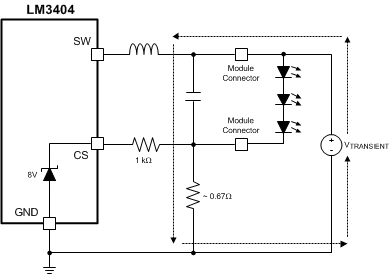 Figure 22. CS Pin, Transient Path With Protection
From measurements, we know that the 8-V ESD structure on the CS pin can typically withstand 25 mA of direct current (DC). Adding a 1-kΩ resistor in series with the CS pin, shown in Figure 22, results in the majority of the transient energy to pass through the discrete sense resistor rather than the device. The series resistor limits the peak current that can flow during a transient event, thus protecting the CS pin. With the 1-kΩ resistor shown, a 33-V, 49-A transient on the LED return connector terminal could be absorbed as calculated by:
This is an extremely high-energy event, so the protection measures previously described should be adequate to solve this issue.
Adding a resistor in series with the CS pin causes the observed output LED current to shift very slightly. The reason for this is twofold: (1) the CS pin has about 20 pF of inherent capacitance inside it, which causes a slight delay (20 ns for a 1-kΩ series resistor), and (2) the comparator that is watching the voltage at the CS pin uses a pnp bipolar transistor at its input. The base current of this pnp transistor is approximately 100 nA which will cause a 0.1-mV change in the 200-mV threshold. These are both very minor changes and are well understood. The shift in current can either be neglected or taken into consideration by changing the current sense resistance slightly.
8.1.8.2 CS Pin Protection With OVP
When designing output overvoltage protection into the switching converter circuit using a Zener diode, transient protection on the CS pin requires additional consideration. As shown in Figure 23, adding a Zener diode from the output to the CS pin (with the series resistor) for output overvoltage protection will now again allow the transient energy to be passed
Adding an additional series resistor to the CS pin as shown in Figure 24 will result in the majority of the transient energy to pass through the sense resistor thereby protecting the LM3404x device.
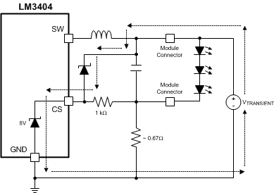 Figure 23. CS Pin With OVP, Transient Path
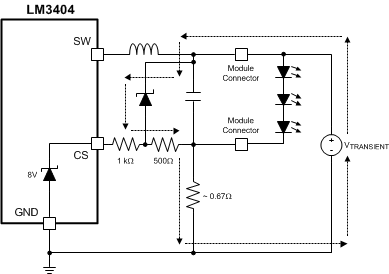 Figure 24. CS Pin With OVP, Transient Path With Protection
8.1.8.3 VIN Pin Protection
The VIN pin also has an ESD structure from the pin to GND with a breakdown voltage of approximately 80 V. Any transient that exceeds this voltage may damage the device. Although transient absorption is usually present at the front end of a switching converter circuit, damage to the VIN pin can still occur.
When VIN is hot swapped in, the current that rushes in to charge CIN up to the VIN value also charges (energizes) the circuit board trace inductance as shown in Figure 25. The excited trace inductance then resonates with the input capacitance (similar to an under-damped LC tank circuit) and causes voltages at the VIN pin to rise well in excess of both VIN and the voltage at the module input connector as clamped by the input TVS. If the resonating voltage at the VIN pin exceeds the 80-V breakdown voltage of the ESD structure, the ESD structure will activate and then snap-back to a lower voltage due to its inherent design. If this lower snap-back voltage is less than the applied nominal VIN voltage, then significant current will flow through the ESD structure resulting in the IC being damaged.
An additional TVS or small Zener diode must be placed as close as possible to the VIN pins of each IC on the board, in parallel with the input capacitor as shown in Figure 26. A minor amount of series resistance in the input line would also help, but would lower overall conversion efficiency. For this reason, NTC resistors are often used as inrush limiters instead.
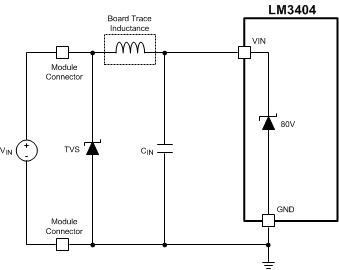 Figure 25. VIN Pin With Typical Input Protection
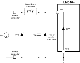 Figure 26. VIN Pin With Additional Input Protection
8.1.8.4 General Comments Regarding Other Pins
Any pin that goes off-board through a connector must have series resistance of at least 1 kΩ to 10 kΩ in series with it to protect it from ESD or other transients. These series resistors limit the peak current that can flow (or cause a voltage drop) during a transient event, thus protecting the pin and the device. Pins that are not used must not be left floating. Instead, the pins must be tied to GND or to an appropriate voltage through resistance.
8.2 Typical Applications
8.2.1 Design Example 1: LM3404
The first example circuit will guide the user through component selection for an architectural accent lighting application. A regulated DC voltage input of 24 V ±10% will power a 5.4-W warm white LED module that consists of four LEDs in a 2 × 2 series-parallel configuration. The module will be treated as a two-terminal element and driven with a forward current of 700 mA ±5%. The typical forward voltage of the LED module in thermal steady state is 6.9 V, hence the average output voltage will be 7.1 V. The objective of this application is to place the complete current regulator and LED module in a compact space formerly occupied by a halogen light source. (The LED will be on a separate metal-core PCB and heatsink.) Switching frequency will be 400 kHz to keep switching loss low, as the confined space with no air-flow requires a maximum temperature rise of 50°C in each circuit component. A small solution size is also important, as the regulator must fit on a circular PCB with a 1.5" diameter. A complete bill of materials can be found in Table 2 at the end of this example.
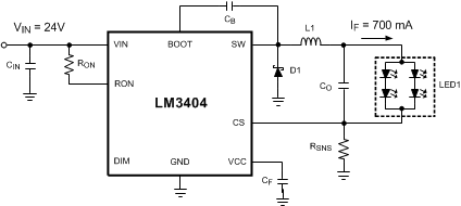 Figure 27. Schematic for Design Example 1
8.2.1.1 Design Requirements
- Input voltage: 24 V ±10%
- LED forward voltage: 6.9 V
- LED current: 700 mA
- Switching frequency: 400 kHz
8.2.1.2 Detailed Design Procedure
8.2.1.2.1 RON and tON
A moderate switching frequency is needed in this application to balance the requirements of magnetics size and efficiency. RON is selected from the equation for switching frequency as shown in Equation 17 and Equation 18.

The closest 1% tolerance resistor is 133 kΩ. The switching frequency and on-time of the circuit can then be found using the equations relating RON and tON to fSW, as shown in Equation 19 and Equation 20
8.2.1.2.2 Output Inductor
Because an output capacitor will be used to filter some of the AC ripple current, the inductor ripple current can be set higher than the LED ripple current. A value of 40%P-P is typical in many buck converters:
With the target ripple current determined the inductance can be chosen:

The closest standard inductor value is 47 µH. The average current rating must be greater than 700 mA to prevent overheating in the inductor. Separation between the LM3404 drivers and the LED arrays means that heat from the inductor will not threaten the lifetime of the LEDs, but an overheated inductor could still cause the LM3404 to enter thermal shutdown.
The inductance of the standard part chosen is ±20%. With this tolerance the typical, minimum, and maximum inductor current ripples can be calculated:
The peak LED/inductor current is then estimated:
In the case of a short circuit across the LED array, the LM3404 will continue to deliver rated current through the short but will reduce the output voltage to equal the CS pin voltage of 200 mV. The inductor ripple current and peak current in this condition would be equal to:
In the case of a short at the switch node, the output, or from the CS pin to ground the short circuit current limit will engage at a typical peak current of 1.5 A. To prevent inductor saturation during these fault conditions the inductor’s peak current rating must be above 1.5 A. A 47-µH off-the shelf inductor rated to 1.4 A (peak) and 1.5 A (average) with a DCR of 0.1 Ω will be used.
8.2.1.2.3 Using an Output Capacitor
This application does not require high frequency PWM dimming, allowing the use of an output capacitor to reduce the size and cost of the output inductor. To select the proper output capacitor, the equation from Buck Converters With Output Capacitors is re-arranged to yield Equation 31.

The target tolerance for LED ripple current is 100 mAP-P, and a typical value for rD is 1.8 Ω at 700 mA. The required capacitor impedance to reduce the worst-case inductor ripple current of 333 mAP-P is therefore:
A ceramic capacitor will be used and the required capacitance is selected based on the impedance at 400 kHz:
This calculation assumes that impedance due to the equivalent series resistance (ESR) and equivalent series inductance (ESL) of CO is negligible. The closest 10% tolerance capacitor value is 1 µF. The capacitor used must be rated to 25 V or more and have an X7R dielectric. Several manufacturers produce ceramic capacitors with these specifications in the 0805 case size. A typical value for ESR is 3 mΩ.
8.2.1.2.4 RSNS
A preliminary value for RSNS was determined in selecting ΔiL. This value must be re-evaluated based on the calculations for ΔiF:

Sub-1-Ω resistors are available in both 1% and 5% tolerance. A 1%, 0.33-Ω device is the closest value, and a 0.33 W, 1206 size device will handle the power dissipation of 162 mW. With the resistance selected, the average value of LED current is re-calculated to ensure that current is within the ±5% tolerance requirement. The average LED current can be found using Equation 36.
8.2.1.2.5 Input Capacitor
Following the calculations from the Input Capacitor section, ΔvIN(MAX) will be 24 V × 2%P-P = 480 mV. The minimum required capacitance is:
To provide additional safety margin the a higher value of 3.3-µF ceramic capacitor rated to 50 V with X7R dielectric in an 1210 case size will be used. From Application Information, input rms current is:
Ripple current ratings for 1210 size ceramic capacitors are typically higher than 2 A, more than enough for this design.
8.2.1.2.6 Recirculating Diode
The input voltage of 24 V ±5% requires Schottky diodes with a reverse voltage rating greater than 30 V. The next highest standard voltage rating is 40 V. Selecting a 40-V rated diode provides a large safety margin for the ringing of the switch node and also makes cross-referencing of diodes from different vendors easier.
The next parameters to be determined are the forward current rating and case size. In this example the low duty cycle (D = 7.1 / 24 = 28%) places a greater thermal stress on D1 than on the internal power MOSFET of the LM3404. The estimated average diode current is:
A Schottky with a forward current rating of 1 A would be adequate, however reducing the power dissipation is critical in this example. Higher current diodes have lower forward voltages, hence a 2-A rated diode will be used. To determine the proper case size, the dissipation and temperature rise in D1 can be calculated as shown in Application Information. VD for a case size such as SMB in a 40 V, 2-A Schottky diode at 700 mA is approximately 0.3 V and the θJA is 75°C/W. Power dissipation and temperature rise can be calculated as:
8.2.1.2.7 CB and CF
The bootstrap capacitor CB must always be a 10-nF ceramic capacitor with X7R dielectric. A 25-V rating is appropriate for all application circuits. The linear regulator filter capacitor CF must always be a 100-nF ceramic capacitor, also with X7R dielectric and a 25-V rating.
8.2.1.2.8 Efficiency
To estimate the electrical efficiency of this example the power dissipation in each current carrying element can be calculated and summed. Electrical efficiency, η, must not be confused with the optical efficacy of the circuit, which depends upon the LEDs themselves.
Total output power, PO, is calculated as:
Conduction loss, PC, in the internal MOSFET:
Gate charging and VCC loss, PG, in the gate drive and linear regulator:
Switching loss, PS, in the internal MOSFET:
AC rms current loss, PCIN, in the input capacitor:
DCR loss, PL, in the inductor
Recirculating diode loss, PD = 153 mW
Current Sense Resistor Loss, PSNS = 164 mW
Electrical efficiency, η = PO / (PO + Sum of all loss terms) = 5 / (5 + 0.687) = 88%
Temperature Rise in the LM3404 IC is calculated as:
8.2.1.3 Application Curves
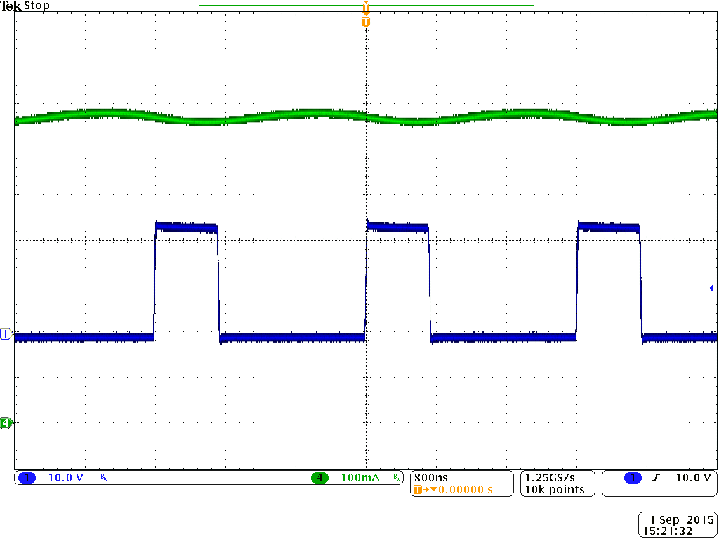 Figure 28. LED Current (green) and SW (blue) Waveforms
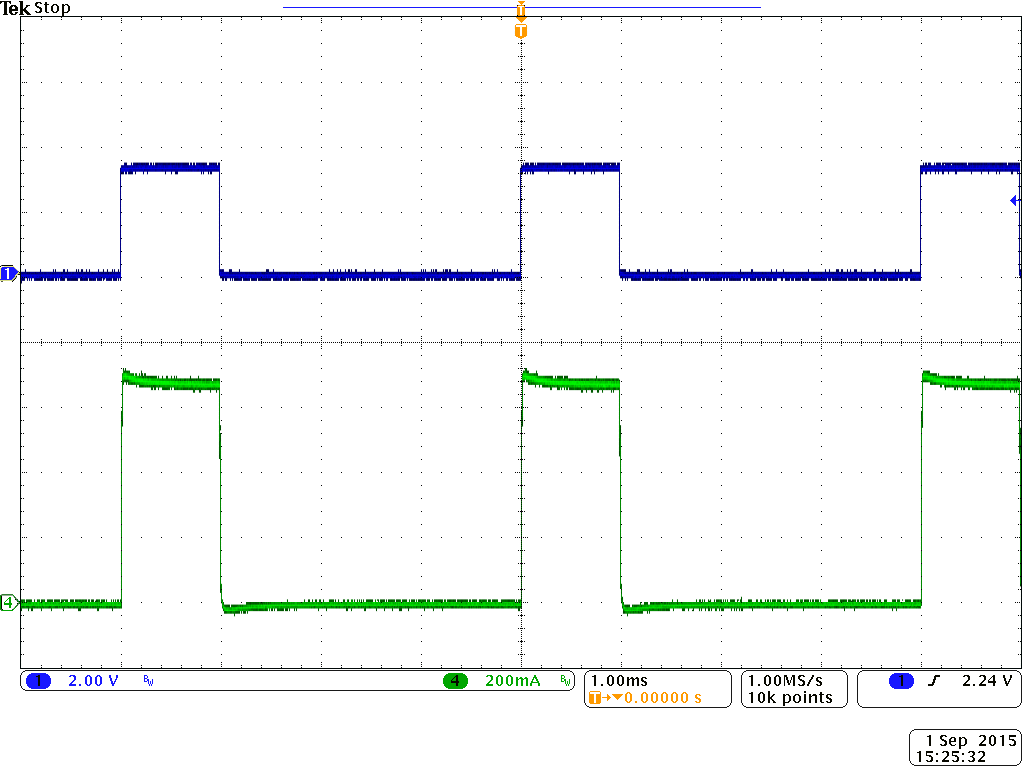 Figure 29. DIM (blue) and LED Current (green) 250Hz PWM Waveforms
Table 2. BOM for Design Example 1
| ID | PART NUMBER | TYPE | SIZE | PARAMETER | QTY | VENDOR |
|---|---|---|---|---|---|---|
| U1 | LM3404 | LED Driver | SOIC-8 | 42 V, 1.2 A | 1 | TI |
| L1 | SLF10145T-470M1R4 | Inductor | 10 × 10 × 4.5 mm | 47 µH, 1.4 A, 120 mΩ | 1 | TDK |
| D1 | CMSH2-40 | Schottky Diode | SMB | 40 V, 2 A | 1 | Central Semi |
| Cf | VJ0805Y104KXXAT | Capacitor | 0805 | 100 nF 10% | 1 | Vishay |
| Cb | VJ0805Y103KXXAT | Capacitor | 0805 | 10 nF 10% | 1 | Vishay |
| Cin | C3225X7R1H335M | Capacitor | 1210 | 3.3 µF, 50V | 1 | TDK |
| Co | C2012X7R1E105M | Capacitor | 0805 | 1 µF, 25V | 1 | TDK |
| Rsns | ERJ8BQFR33V | Resistor | 1206 | 0.33 Ω 1% | 1 | Panasonic |
| Ron | CRCW08051333F | Resistor | 0805 | 133 kΩ 1% | 1 | Vishay |
8.2.2 Design Example 2: LM3404HV
The second example circuit will guide the user through component selection for an outdoor general lighting application. A regulated DC voltage input of 48 V ±10% will power ten series-connected LEDs at 500 mA ±10% with a ripple current of 50 mAP-P or less. The typical forward voltage of the LED module in thermal steady state is 35 V, hence the average output voltage will be 35.2 V. A complete bill of materials can be found in Table 3.
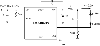 Figure 30. Schematic for Design Example 2
8.2.2.1 Design Requirements
- Input voltage: 48 V ±10%
- LED forward voltage: 35 V
- LED current: 500 mA
- Switching frequency: 225 kHz
8.2.2.2 Detailed Design Procedure
8.2.2.2.1 RON and tON
A low switching frequency, 225 kHz, is needed in this application, as high-efficiency and low-power dissipation take precedence over the solution size. RON is selected from the equation for switching frequency as shown in Equation 50 and Equation 51.

The next highest 1% tolerance resistor is 1.18 MΩ. The switching frequency and on-time of the circuit can then be found using the equations relating RON and tON to fSW, as shown in Equation 52 and Equation 53.
8.2.2.2.2 Output Inductor
Because an output capacitor will be used to filter some of the AC ripple current, the inductor ripple current can be set higher than the LED ripple current. A value of 30%P-P makes a good trade-off between the current ripple and the size of the inductor:
With the target ripple current determined the inductance can be chosen:

The closest standard inductor value above 281 is 330 µH. The average current rating must be greater than 0.5 A to prevent overheating in the inductor. In this example the LM3404HV driver and the LED array share the same metal-core PCB, meaning that heat from the inductor could threaten the lifetime of the LEDs. For this reason the average current rating of the inductor used must have a derating of about 50%, or 1 A.
The inductance of the standard part chosen is ±20%. With this tolerance the typical, minimum, and maximum inductor current ripples can be calculated:
The peak inductor current is then estimated:
In the case of a short circuit across the LED array, the LM3404HV will continue to deliver rated current through the short but will reduce the output voltage to equal the CS pin voltage of 200 mV. The inductor ripple current and peak current in this condition would be equal to:
In the case of a short at the switch node, the output, or from the CS pin to ground the short circuit current limit will engage at a typical peak current of 1.5 A. To prevent inductor saturation during these fault conditions the inductor’s peak current rating must be above 1.5 A. A 330-µH off-the shelf inductor rated to 1.9 A (peak) and 1 A (average) with a DCR of 0.56 Ω will be used.
8.2.2.2.3 Using an Output Capacitor
This application uses sub-1 kHz frequency PWM dimming, allowing the use of a small output capacitor to reduce the size and cost of the output inductor. To select the proper output capacitor, the equation from buck regulators with output capacitors is re-arranged to yield Equation 64.

The target tolerance for LED ripple current is 50 mAP-P, and the typical value for rD is 10 Ω with ten LEDs in series. The required capacitor impedance to reduce the worst-case steady-state inductor ripple current of 160 mAP-P is therefore:
A ceramic capacitor will be used and the required capacitance is selected based on the impedance at 223 kHz:
This calculation assumes that impedance due to the equivalent series resistance (ESR) and equivalent series inductance (ESL) of CO is negligible. The closest 10% tolerance capacitor value is 0.15 µF. The capacitor used must be rated to 50 V or more and have an X7R dielectric. Several manufacturers produce ceramic capacitors with these specifications in the 0805 case size. ESR values are not typically provided for such low value capacitors, however is can be assumed to be under 100 mΩ, leaving plenty of margin to meet to LED ripple current requirement. The low capacitance required allows the use of a 100-V rated, 1206-size capacitor. The rating of 100 V ensures that the capacitance will not decrease significantly when the DC output voltage is applied across the capacitor.
8.2.2.2.4 RSNS
A preliminary value for RSNS was determined in selecting ΔiL. This value must be re-evaluated based on the calculations for ΔiF:

Sub-1-Ω resistors are available in both 1% and 5% tolerance. A 1%, 0.43-Ω device is the closest value, and a 0.25 W, 0805 size device will handle the power dissipation of 110 mW. With the resistance selected, the average value of LED current is re-calculated to ensure that current is within the ±10% tolerance requirement. The average LED current can be found using Equation 69.
8.2.2.2.5 Input Capacitor
Following the calculations from the Input Capacitor section, ΔvIN(MAX) will be 48 V × 2%P-P = 960 mV. The minimum required capacitance is:
To provide additional safety margin a 2.2-µF ceramic capacitor rated to 100 V with X7R dielectric in an 1812 case size will be used. From Application Information, input rms current is:
Ripple current ratings for 1812 size ceramic capacitors are typically higher than 2 A, more than enough for this design, and the ESR is approximately 3 mΩ.
8.2.2.2.6 Recirculating Diode
The input voltage of 48 V requires Schottky diodes with a reverse voltage rating greater than 50 V. The next highest standard voltage rating is 60 V. Selecting a 60-V rated diode provides a large safety margin for the ringing of the switch node and also makes cross-referencing of diodes from different vendors easier.
The next parameters to be determined are the forward current rating and case size. In this example the high duty cycle (D = 35.2 / 48 = 73%) places a greater thermal stress on the internal power MOSFET than on D1. The estimated average diode current is:
A Schottky with a forward current rating of 0.5 A would be adequate; however, reducing the power dissipation is critical in this example. Higher current diodes have lower forward voltages, hence a 1-A rated diode will be used. To determine the proper case size, the dissipation and temperature rise in D1 can be calculated as shown in Application Information. VD for a case size such as SMA in a 60-V, 1-A Schottky diode at 0.5 A is approximately 0.35 V and the θJA is 75°C/W. Power dissipation and temperature rise can be calculated as:
8.2.2.2.7 CB and CF
The bootstrap capacitor CB must always be a 10-nF ceramic capacitor with X7R dielectric. A 25-V rating is appropriate for all application circuits. The linear regulator filter capacitor CF must always be a 100-nF ceramic capacitor, also with X7R dielectric and a 25-V rating.
8.2.2.2.8 Efficiency
To estimate the electrical efficiency of this example the power dissipation in each current carrying element can be calculated and summed. Electrical efficiency, η, must not be confused with the optical efficacy of the circuit, which depends upon the LEDs themselves.
Total output power, PO, is calculated as:
Conduction loss, PC, in the internal MOSFET:
Gate charging and VCC loss, PG, in the gate drive and linear regulator:
Switching loss, PS, in the internal MOSFET:
AC rms current loss, PCIN, in the input capacitor:
DCR loss, PL, in the inductor
Recirculating diode loss, PD = 47 mW
Current Sense Resistor Loss, PSNS = 110 mW
Electrical efficiency, η = PO / (PO + Sum of all loss terms) = 17.6 / (17.6 + 0.644) = 96%
Temperature Rise in the LM3404HV IC is calculated as:
8.2.2.3 Application Curves
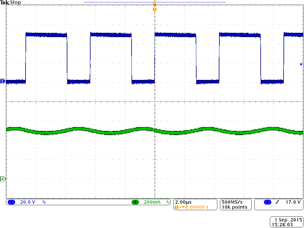 Figure 31. LED Current (Green) and SW (Blue) Waveforms
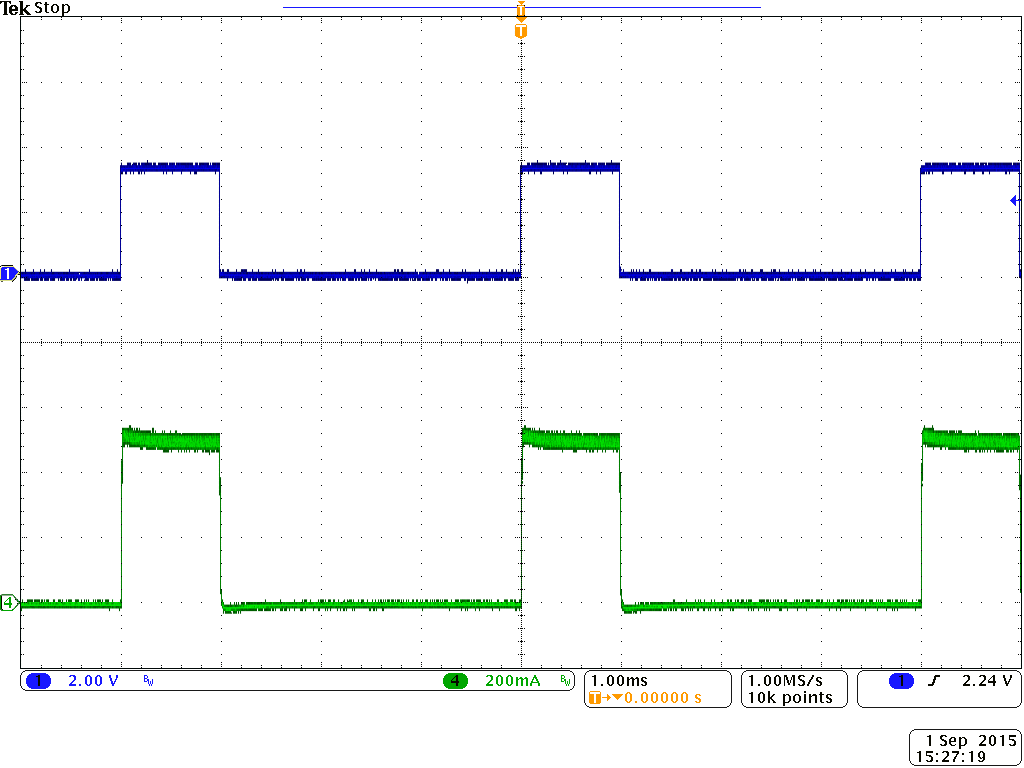 Figure 32. DIM (Blue) and LED Current (Green) 250Hz PWM Waveforms