6 Specifications
6.1 Absolute Maximum Ratings
over operating free-air temperature range (unless otherwise noted)(1)(2)(3)
|
MIN |
MAX |
UNIT |
| VIN to GND |
–0.3 |
6 |
V |
| VOUT, LED−, FB to GND |
–0.3 |
6 |
V |
| SDA, SCL, STROBE, FET_CON, EOC, ALD/TEMP, IND to GND |
–0.3 |
6 |
V |
| Continuous power dissipation(4) |
Internally limited |
|
| Junction temperature, TJ-MAX |
|
150 |
°C |
| Storage temperature, Tstg |
–65 |
150 |
°C |
(1) Stresses beyond those listed under
Absolute Maximum Ratings may cause permanent damage to the device. These are stress ratings only, which do not imply functional operation of the device at these or any other conditions beyond those indicated under
Recommended Operating Conditions. Exposure to absolute-maximum-rated conditions for extended periods may affect device reliability.
(2) All voltages are with respect to the potential at the GND pin.
(3) If Military/Aerospace specified devices are required, contact the Texas Instruments Sales Office/ Distributors for availability and specifications.
(4) Internal thermal shutdown circuitry protects the device from permanent damage. Thermal shutdown engages at TJ = 145°C (typical) and disengages at TJ = 125°C (typical). The thermal shutdown is specified by design.
6.2 ESD Ratings
|
VALUE |
UNIT |
| V(ESD) |
Electrostatic discharge |
Human-body model (HBM), per ANSI/ESDA/JEDEC JS-001(1) |
±2000 |
V |
| Machine model(2) |
±200 |
(1) JEDEC document JEP155 states that 500-V HBM allows safe manufacturing with a standard ESD control process.
(2) The LED pin has a machine model ESD rating of 150 V.
6.3 Recommended Operating Conditions
over operating free-air temperature range (unless otherwise noted)(1)
|
MIN |
NOM |
MAX |
UNIT |
| Input voltage |
2.7 |
|
5.5 |
V |
| Junction temperature, TJ |
–30 |
|
125 |
°C |
| Ambient temperature, TA |
–30 |
|
85 |
°C |
(1) All voltages are with respect to the potential at the GND pin.
6.4 Thermal Information
| THERMAL METRIC(1) |
LM3550 |
UNIT |
| NHU (UQFN) |
| 16 PINS |
| RθJA |
Junction-to-ambient thermal resistance |
60.1 |
°C/W |
| RθJC(top) |
Junction-to-case (top) thermal resistance |
30.5 |
°C/W |
| RθJB |
Junction-to-board thermal resistance |
28.1 |
°C/W |
| ψJT |
Junction-to-top characterization parameter |
0.7 |
°C/W |
| ψJB |
Junction-to-board characterization parameter |
28.3 |
°C/W |
| RθJC(bot) |
Junction-to-case (bottom) thermal resistance |
17.8 |
°C/W |
6.5 Electrical Characteristics
Typical imits are for TJ = 25°C; minimum and maximum limits apply over the full ambient junction temperature range (−30°C ≤ TA ≤ 85°C). Unless otherwise noted, specifications apply to Typical Application with: : VIN = 3.6 V, CIN = 4.7 µF, COUT = 2.2 µF, C1 = C2 = 1 µF.(1)(2)
| PARAMETER |
TEST CONDITION |
MIN(3) |
TYP |
MAX(3) |
UNIT |
| ILED– |
Current sink accuracy |
2.7 V ≤ VIN ≤ 5.5 V
3 V ≤ VIN ≤ 5.5 V |
54 |
60 |
66 |
mA |
| 90 |
100 |
110 |
| 180 |
200 |
220 |
| VOVP |
Output overvoltage protection |
2.7 V ≤ VIN ≤ 5.5 V |
Going into OVP |
|
5.3 |
5.479 |
V |
| Hysteresis |
|
0.2 |
|
| VOUT |
Output voltage regulation |
2.7 V ≤ VIN ≤ 5.5 V, IOUT = 0 mA |
4.275 |
4.5 |
4.666 |
V |
| 4.75 |
5 |
5169 |
| 5.035 |
5.3 |
5.479 |
| VBAL |
BAL pin voltage regulation |
2.7 V ≤ VIN ≤ 5.5 V |
|
VOUT / 2 |
|
|
| IIND |
IND pin current regulation |
2.7 V ≤ VIN ≤ 5.5 V, VIND = 2 V |
3.3 |
4.8 |
6.3 |
mA |
| ƒSW |
Switching frequency |
2.7 V ≤ VIN ≤ 5.5 V |
0.882 |
1 |
1.153 |
MHz |
| VFB |
FEEDBACK pin regulation voltage |
2.7 V ≤ VIN ≤ 5.5 V, VOUT = 4.6 V |
94 |
100 |
106 |
mV |
| VALD/TEMP |
ALD/TEMP pin reference voltage |
2.7 V ≤ VIN ≤ 5.5 V |
095 |
1 |
1.05 |
V |
| VEOC |
EOC pin output logic load |
ILOAD = 3 mA |
|
|
400 |
mV |
| IIN-CL |
Input current limit |
VOUT = 0 V |
|
534 |
610 |
mA |
| ISD |
Shutdown supply current |
Device disabled, 2.7 V ≤ VIN ≤ 5.5 V |
|
1.8 |
4 |
µA |
| IQ |
Quiescent supply current |
2.7 V ≤ VIN ≤ 5.5 V, IOUT = 0 mA
5-V charge mode, non switching |
|
168 |
240 |
µA |
| VSTROBE |
STROBE logic thresholds |
2.7 V ≤ VIN ≤ 5.5 V |
High |
1.23 |
|
VIN |
V |
| Low |
0 |
|
0.7 |
| I2C-COMPATIBLE VOLTAGE SPECIFICATIONS (SCL, SDA) |
| VIL |
Input logic low |
2.7 V ≤ VIN ≤ 5.5 V |
0 |
|
0.7 |
V |
| VIH |
Input logic high |
2.7 V ≤ VIN ≤ 5.5 V |
1.23 |
|
VIN |
V |
| VOL |
Output logic low |
ILOAD = 3 mA |
|
|
400 |
mV |
(1) All voltages are with respect to the potential at the GND pin.
(2) Junction-to-ambient thermal resistance (RθJA) is taken from a thermal modeling result, performed under the conditions and guidelines set forth in the JEDEC standard JESD51-7. The test board is a 4-layer FR-4 board measuring 102 mm × 76 mm × 1.6 mm with a 2 × 1 array of thermal vias. The ground plane on the board is 50 mm x 50 mm. Thickness of copper layers are 36 µm/18 µm/18 µm/36 µm (1.5oz/1oz/1oz/1.5oz). Ambient temperature in simulation is 22°C, still air. Power dissipation is 1 W.
(3) Minimum (MIN) and maximum (MAX) limits are specified by design, test, or statistical analysis. Typical (TYP) numbers are not ensured, but do represent the most likely norm. Unless otherwise specified, conditions for TYP specifications are: VIN = 3.6 V and TA = 25°C.
6.6 Timing Requirements
| |
MIN |
NOM |
MAX |
UNIT |
| t1 |
SCK (clock period) |
294 |
|
|
ns |
| t2 |
Data in setup time to SCL high, ƒSCL = 400 kHz |
100 |
|
|
ns |
| t3 |
Data out stable after SCL low, ƒSCL = 400 kHz |
0 |
|
|
ns |
| t4 |
SDA low setup time to SCL low (start), fSCL = 400 kHz |
100 |
|
|
ns |
| t5 |
SDA igh hold time after SCL high (stop), fSCL = 400 kHz |
100 |
|
|
ns |
 Figure 1. LM3550 Timing
6.7 Typical Characteristics
Unless otherwise specified: TA = 25°C; VIN = 3.6 V; CIN = 4.7 µF, COUT = 2.2 µF, C1 = C2 = 1 µF. Super capacitor = 0.5 F TDK EDLC272020-501-2F-50.
 Figure 2. Output Voltage vs Output Current
 Figure 4. Output Voltage vs Output Current
 Figure 3. Output Voltage vs Output Current
 Figure 5. Output Voltage vs Output Current
 Figure 6. Output Voltage vs Output Current
 Figure 8. Input Current Limit vs Output Voltage
 Figure 10. Converter Efficiency vs Input Voltage
 Figure 12. Torch Current vs Input Voltage Code = 0
 Figure 14. Torch Current vs Input Voltage Code = 2
 Figure 16. Torch Current vs Input Voltage Code = 4
 Figure 18. Torch Current vs Input Voltage Code = 6
 Figure 20. Torch Current vs Input Voltage Different VLED
 Figure 22. Oscillator Frequency vs Input Voltage
 Figure 24. Indicator Current vs Input Voltage Different VLED
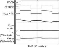
 Figure 26. 5.3-V Mode Super Capacitor Charge
 Figure 28. 5.3-V Mode Super Capacitor Recharge
 Figure 30. Edge-Sensitive Strobe
 Figure 32. Flash With FGATE = 0
 Figure 34. ALS Detect Zone 0
 Figure 36. ALS Detect Zone 2
 Figure 7. Output Voltage vs Output Current
 Figure 9. Input Current Limit vs Output Voltage Tri-Temp
 Figure 11. Torch Current vs Brightness Code
 Figure 13. Torch Current vs Input Voltage Code = 1
 Figure 15. Torch Current vs Input Voltage Code = 3
 Figure 17. Torch Current vs Input Voltage Code = 5
 Figure 19. Torch Current vs Input Voltage Code = 7
 Figure 21. Feedback Voltage vs Input Voltage
 Figure 23. Shutdown Current vs Input Voltage
 Figure 25. Indicator Current vs Input Voltage Tri-Temp
 Figure 27. 2 LED, 3-A Flash (1.5 A Each)
 Figure 29. Strobe-to-Flash Delay
 Figure 31. Level-Sensitive Strobe
 Figure 33. Flash With FGATE = 1
 Figure 35. ALS Detect Zone 1
 Figure 1. LM3550 Timing


