SNVS594G December 2008 – April 2016 LM3555
PRODUCTION DATA.
- 1 Features
- 2 Applications
- 3 Description
- 4 Revision History
- 5 Pin Configuration and Functions
- 6 Specifications
-
7 Detailed Description
- 7.1 Overview
- 7.2 Functional Block Diagram
- 7.3 Feature Description
- 7.4 Device Functional Modes
- 7.5 Programming
- 7.6 Register Maps
- 8 Application and Implementation
- 9 Power Supply Recommendations
- 10Layout
- 11Device and Documentation Support
- 12Mechanical, Packaging, and Orderable Information
Package Options
Mechanical Data (Package|Pins)
- YZR|12
Thermal pad, mechanical data (Package|Pins)
Orderable Information
8 Application and Implementation
NOTE
Information in the following applications sections is not part of the TI component specification, and TI does not warrant its accuracy or completeness. TI’s customers are responsible for determining suitability of components for their purposes. Customers should validate and test their design implementation to confirm system functionality.
8.1 Application Information
The LM3555 is a white-LED driver for LED camera flash applications. The dual high-side current sources allow for grounded cathode LEDs. The LM3555 can adaptively scale the maximum flash level delivered to the LEDs based upon the flash configuration, whether it be a single LED or two LEDs in series.
8.2 Typical Application
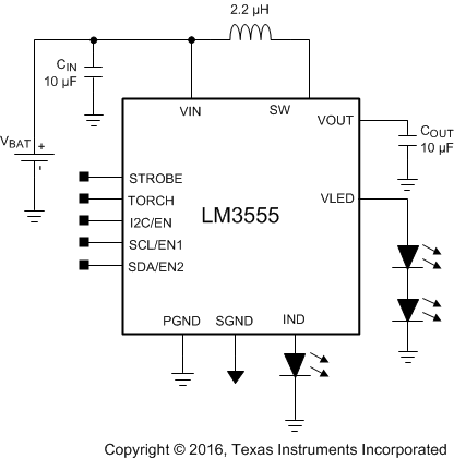 Figure 50. LM3555 Typical Application
8.2.1 Design Requirements
For typical white-LED driver applications, use the parameters listed in Table 10.
Table 10. Design Parameters
| DESIGN PARAMETER | EXAMPLE VALUE |
|---|---|
| Input voltage range | 2.5 V to 5.5 V |
| Number of LEDs | 1 or 2 LEDs in Series |
| Output current range | 60 mA to 500mA |
8.2.2 Detailed Design Procedure
8.2.2.1 Inductor Current Limit
To prevent damage to the inductor of the LM3555 and to limit the power drawn by the LM3555 during a flash event, an inductor current limit circuit is present. The LM3555 monitors the current through the inductor during the charge phase of the boost cycle. In the event that the inductor current reaches the current limit, the NFET of the converter terminates the charge phase for that cycle. The process repeats itself until the flash event has ended or until the input voltage increases to the point where the peak current is no longer reached. Hitting the peak inductor current limit does not disable the part. It does, however, limit the output power delivery to the LEDs.
In simple control mode, the peak inductor current limit is set to 1.75 A. In I2C control mode, the inductor current limit can be set to 1.25 A, 1.5 A, 1.75 A, and 2 A depending on the values of the IL1 and IL0 bits in the Control Register (address 0x04). The peak inductor current limit value can be used to help size the inductor to the appropriate saturation current level. For more information on inductor sizing, please refer to the Inductor Selection.
8.2.2.2 Inductor Selection
The LM3555 is designed to use a 2.2-µH inductor. When the device is boosting (VOUT > VIN) the inductor is one of the biggest sources of efficiency loss in the circuit. Therefore, choosing an inductor with the lowest possible series resistance is important. Additionally, the saturation rating of the inductor must be greater than the maximum operating peak current of the LM3555. This prevents excess efficiency loss that can occur with inductors that operate in saturation and prevents over heating of the inductor and possible damage. For proper inductor operation and circuit performance ensure that the inductor saturation and the peak current limit setting of the LM3555 (1.25 A, 1.5 A, 1.75 A, or 2 A) is greater than IPEAK. IPEAK can be calculated by:

Table 11. Recommended Inductors
| MANUFACTURER | PART NUMBER | L / ISAT |
|---|---|---|
| Toko | FDSE312-2R2M | 2.2 µH / 2.3 A |
| Coilcraft | LPS4012-222ML | 2.2 µH / 2.3 A |
| TDK | VLF4014ST-2R2M1R9 | 2.2 µH / 2 A |
8.2.2.3 Capacitor Selection
The LM3555 requires 2 external capacitors for proper operation (TI recommends CIN = 10 µF (4.7 µF minimum) and COUT = 10 µF ). TI also recommends placing an additional 0.1-µF input capacitor placed right next to the VIN pin. Surface-mount multi-layer ceramic capacitors are recommended. These capacitors are small, inexpensive and have very low equivalent series resistance (ESR < 20 mΩ typical). Tantalum capacitors, OS-CON capacitors, and aluminum electrolytic capacitors are not recommended for use with the LM3555 due to their high ESR, as compared to ceramic capacitors.
For most applications, ceramic capacitors with X7R or X5R temperature characteristic are preferred for use with the LM3555. These capacitors have tight capacitance tolerance (as good as ±10%) and hold their value over temperature (X7R: ±15% over −55°C to +125°C; X5R: ±15% over −55°C to 85°C).
Capacitors with Y5V or Z5U temperature characteristic are generally not recommended for use with the LM3555. Capacitors with these temperature characteristics typically have wide capacitance tolerance (80%, −20%) and vary significantly over temperature (Y5V: 22%, –82% over −30°C to +85°C range; Z5U: 22%, –56% over 10°C to 85°C range). Under some conditions, a nominal 1-µF Y5V or Z5U capacitor could have a capacitance of only 0.1 µF. Such detrimental deviation is likely to cause Y5V and Z5U capacitors to fail to meet the minimum capacitance requirements of the LM3555.
The recommended voltage rating for the input capacitor is 10 V (minimum = 6.3 V). The recommended output capacitor voltage rating is 16 V (minimum = 10 V). The recommended value takes into account the DC bias capacitance losses, while the minimum rating takes into account the OVP trip levels.
8.2.3 Application Curves
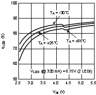
| Two Series LEDs at 320 mA |
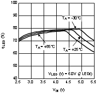
| Two LEDs at 60 mA |
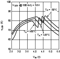
| One LED at 500 mA |
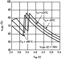
| One LED at 80 mA |
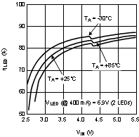
| Two Series LEDs at 400 mA |
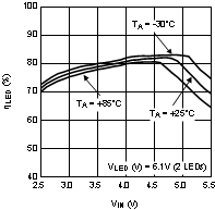
| Two LEDs at 80 mA |
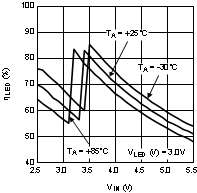
| One LED at 60 mA |