SNVSA63A April 2015 – September 2015 LM3632A
PRODUCTION DATA.
- 1 Features
- 2 Applications
- 3 Description
- 4 Revision History
- 5 Pin Configuration and Functions
- 6 Specifications
-
7 Detailed Description
- 7.1 Overview
- 7.2 Functional Block Diagram
- 7.3
Features Description
- 7.3.1 Backlight
- 7.3.2 LCM Bias
- 7.3.3 Flash
- 7.3.4 Software RESET
- 7.3.5 EN Input
- 7.3.6 Thermal Shutdown (TSD)
- 7.4 Device Functional Modes
- 7.5 Programming
- 7.6
Register Maps
- 7.6.1 Revision (Address = 0x01) [reset = 0x09]
- 7.6.2 Backlight Configuration1 (Address = 0x02) [reset = 0x30]
- 7.6.3 Backlight Configuration2 (Address = 0x03) [reset = 0x0D]
- 7.6.4 Backlight Brightness LSB (Address = 0x04) [reset = 0x07]
- 7.6.5 Backlight Brightness MSB (Address = 0x05) [reset = 0xFF]
- 7.6.6 Flash/Torch Current (Address = 0x06) [reset = 0x3E]
- 7.6.7 Flash Configuration (Address = 0x07) [reset = 0x2F]
- 7.6.8 VIN Monitor (Address = 0x08) [reset = 0x03]
- 7.6.9 I/O Control (Address = 0x09) [reset = 0x00]
- 7.6.10 Enable (Address = 0x0A) [reset = 0x00]
- 7.6.11 Flags1 (Address = 0x0B) [reset = 0x00]
- 7.6.12 Display Bias Configuration (Address = 0x0C) [reset = 0x18]
- 7.6.13 LCM Boost Bias (Address = 0x0D) [reset = 0x1E]
- 7.6.14 VPOS Bias (Address = 0x0E) [reset = 0x1E]
- 7.6.15 VNEG Bias (Address = 0x0F) [reset = 0x1C]
- 7.6.16 Flags2 (Address = 0x10) [reset = 0x00]
- 8 Application and Implementation
- 9 Power Supply Recommendations
- 10Layout
- 11Device and Documentation Support
- 12Mechanical, Packaging, and Orderable Information
Package Options
Mechanical Data (Package|Pins)
- YFF|30
Thermal pad, mechanical data (Package|Pins)
Orderable Information
7 Detailed Description
7.1 Overview
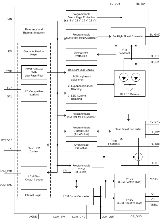
The LM3632A is a single-chip complete backlight, LCM power and flash solution. The device operates over the 2.7-V to 5-V input voltage range.
The LM3632A can drive up to two LED strings with up to 8 LEDs each (up to 28 V typical), with a maximum of 25 mA per string. The power for the LED strings comes from a integrated asynchronous backlight boost converter with two selectable switching frequencies to optimize performance or solution area. LED current is regulated by two low-headroom current sinks. Automatic voltage scaling adjusts the output voltage of the backlight boost converter to minimize the LED driver headroom voltage. The 11-bit LED current is set via an I2C interface, via a logic level PWM input, or a combination of both.
The LCM bias power portion of the LM3632A consists of a synchronous LCM bias boost converter, inverting charge pump, and an integrated LDO. The LCM positive bias voltage VPOS (up to 6 V) is post-regulated from the LCM bias boost converter output voltage. The LCM negative bias voltage VNEG (down to –6 V) is generated from the LCM bias boost converter output using a regulated inverting charge pump.
The flash driver consists of a synchronous boost converter and a 1.5-A constant current LED driver. The high-side current source allows for grounded cathode LED operation providing flash current up to 1.5 A. An adaptive regulation method ensures the current source remains in regulation and maximizes efficiency.
The LM3632A flexible control interface consists of an EN active low reset input, LCM_EN1 and LCM_EN2 inputs for VPOS and VNEG enable control, PWM input for content adaptive backlight control (CABC), a TX flash interrupt input, and an I2C-compatible interface.
Additionally, there are two flag registers with flag and status bits. The user can read back these registers and determine if a fault or warning message has been generated.
7.2 Functional Block Diagram
7.3 Features Description
7.3.1 Backlight
The backlight is enabled if the BL_EN bit (bit[0] in reg[0x0A]) is set to ‘1’, at least one of the backlight sink outputs is enabled (bit[3] and/or bit[4] in reg[0x0A]), and the brightness value is different than 0. When the brightness value is 0 or the BL_EN bit is ‘0’, the backlight is disabled.
7.3.1.1 Brightness Control
Brightness can be controlled either by the I2C brightness register or a combination of the external PWM control and the I2C brightness register. The backlight truth table is shown in Table 1.
When controlling brightness through I2C, registers 0x04 and 0x05 are used. Registers 0x04 and 0x05 hold the 11-bit brightness data. Register 0x04 contains the 3 LSBs, and register 0x05 contains the 8 MSBs. The LED current transitions to the new level after a write is done to register 0x05.
When controlling brightness through I2C, setting the brightness value to '0' shuts down the backlight. When controlling the brightness with PWM input, if PWM input is low for a certain period of time (25 ms typ.), the backlight shuts down. When using the combination of a PWM input and the I2C register, either option shuts down the backlight.
Table 1. Backlight Truth Table
| EN PIN | BL_EN 0x0A[0] |
BLED1_EN 0x0A[4] |
BLED2_EN 0x0A[3] |
PWM_EN 0x09[6] |
ACTION |
|---|---|---|---|---|---|
| 0 | X | X | X | X | Shutdown |
| 1 | 0 | X | X | X | Standby |
| 1 | 1 | 0 | 0 | X | Bias enable |
| 1 | 1 | 1 | 0 | 0 | BLED1 ramp to target current |
| 1 | 1 | 0 | 1 | 0 | BLED1 & BLED2 ramp-to-target current |
| 1 | 1 | 1 | 1 | 0 | BLED1 & BLED2 ramp-to-target current |
| 1 | 1 | 1 | 0 | 1 | BLED1 ramp to (target current × PWM duty cycle) |
| 1 | 1 | 0 | 1 | 1 | BLED1 & BLED2 ramp to (target current × PWM duty cycle) |
| 1 | 1 | 1 | 1 | 1 | BLED1 & BLED2 ramp to (target current × PWM duty cycle) |
7.3.1.1.1 LED Current with PWM Disabled
When LED brightness is controlled from the I2C brightness registers, the 11-bit brightness data directly controls the LED current in BLED1 and BLED2. LED mapping can be selected as either linear or exponential. When this mode is selected, setting the PWM input to 0 does not disable the backlight.
With exponential mapping the 11-bit code-to-current response is approximated by the equation:
Equation 1 is valid for I2C brightness codes between 1 and 2047. Code 0 disables the backlight. The Code-to-LED current response realizes a 0.304% change in LED current per LSB of brightness code.
Figure 22 and Figure 23 detail the exponential response of the LED current vs. brightness code. Figure 22 shows the response on a linear Y axis while Figure 23 shows the response on a log Y axis to show the low current levels at the lower codes.
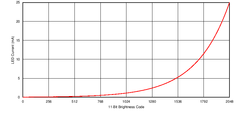 Figure 22. Exponential Response of LED Current vs Brightness Code
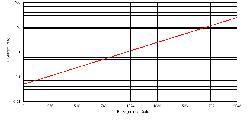 Figure 23. Response of LED Current vs Brightness Code on a Log Y Axis
With linear mapping the 11-bit code to current response is approximated by the equation:
Equation 2 is valid for codes between 1 and 2047. Code 0 disables the backlight.
7.3.1.1.2 LED Current with PWM Enabled
When LED brightness is controlled with the combination of I2C register and the PWM duty cycle, the multiplication result of I2C register value and PWM duty cycle controls the LED current in BLED1 and BLED2. LED mapping can be selected as either linear or exponential.
With exponential mapping the multiplication result-to-current response is approximated by the equation:
Equation 3 is valid for brightness values other than 0. Brightness value 0 (PWM D/C or I2C BRGT CODE) disables the backlight.
With linear mapping the PWM duty cycle-to-current response is approximated by the equation:
Equation 4 is valid for brightness values other than 0. Brightness value 0 (PWM D/C or I2C BRGT CODE) disables the backlight.
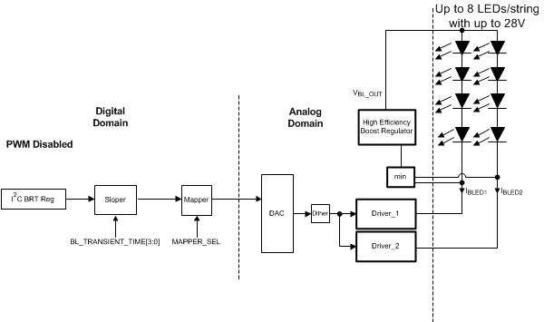 Figure 24. Brightness Control with PWM Bit Disabled
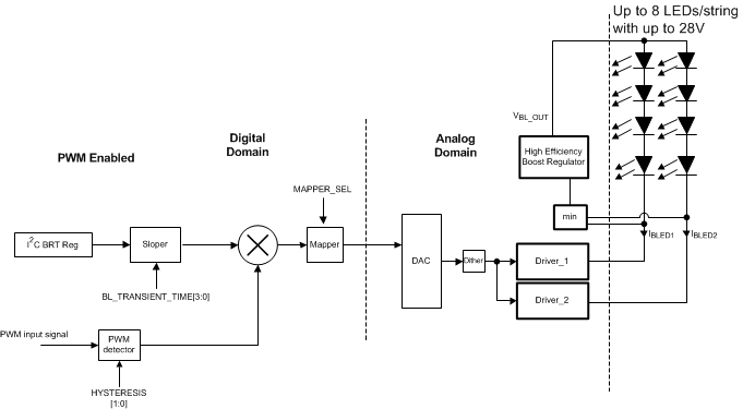 Figure 25. Brightness Control with PWM Bit Enabled
7.3.1.2 Sloper
The sloper smooths the transition from one brightness value to another. Slope time can be adjusted from 0 ms to 8000 ms with BL_TRANS[3:0] bits (see Table 9 for details). Transient time is used for sloping up and down. Transient time always remains the same regardless of the amount of change in brightness.
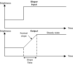 Figure 26. Sloper
7.3.1.3 Mapper
The mapper block maps the digital word set for the LED driver into current code. The user can select whether the mapping is exponential or linear with the BLED_MAP bit, register 0x02 bit[4].
Exponential control is tailored to the response of the human eye such that the perceived change in brightness during ramp up or ramp down is linear.
7.3.1.4 PWM Input
The PWM detector block measures the duty cycle in the PWM pin. The PWM period is measured from the rising edge to the next rising edge. PWM polarity can be changed with bit PWM_CONFIG, register 0x02 bit[3]. The sample rate for the PWM input can be set to 1 MHz or 4 MHz with bit PWM_FREQ, register 0x03 bit[2]. The choice of sample rate depends on three factors:
- Required PWM resolution (input duty cycle to brightness code, with 11 bits max)
- PWM input frequency
- Efficiency
The PWM input block timeout is 25 ms for 1-MHz sampling frequency and 3 ms for 4-MHz sampling frequency, measured from the last rising edge. This should be taken into account for 0% and 100% brightness settings (for setting 100% brightness, the high level of PWM input signal should be greater than the PWM input timeout) and for selecting the minimum PWM input signal frequency.
7.3.1.5 PWM Minimum On/Off Time
The minimum PWM input signal allowed for low and high pulse width is 6 µs for 1-MHz sampling frequency and 1.5 µs for 4-MHz sampling frequency. This should be taken into account when selecting the PWM input signal frequency and maximum or minimum duty cycle. For example, if the PWM input signal frequency is 2 kHz (500 µs) and the 4-MHz sampling frequency is used, the maximum allowed on-time is: (500 – 1.5) µs = 498.5 µs. The maximum duty cycle allowed is 100 × (498.5/500) = 99.7%. By comparison, following similar calculations, with a PWM input signal frequency of 20 kHz the maximum allowed duty cycle is 97%.
NOTE
If the Minimum Off Time requirement is violated, there may be a range of duty cycle values in which flickering of the LEDs may occur or the LEDs may turn off completely. As the duty cycle increases farther and approaches 100%, the LEDs will turn on at full brightness level. This is due to the algorithm used by the device to detect 100% duty cycle in conjunction with the minimum low pulse width requirement discussed in this section. To avoid LED flickering and/or the LEDs turning off at high PWM duty cycles, the PWM Minimum On/Off Time requirement should be met.
7.3.1.6 PWM Resolution and Input Frequency Range
The PWM input resolution depends on the input signal frequency. To achieve the full 11-bit maximum resolution of PWM duty cycle to the LED brightness code, the input PWM duty cycle must be ≥ 11 bits, and the PWM sample period (1/fSAMPLE) must be smaller than the minimum PWM input pulse width. Figure 27 shows the possible brightness code resolutions based on the input PWM frequency. The minimum recommended PWM frequency is 100 Hz, and maximum recommended PWM frequency is 20 kHz.
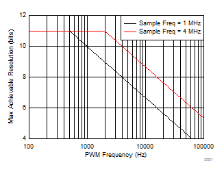 Figure 27. PWM Resolution and PWM Input Frequency
7.3.1.7 PWM Hysteresis
To prevent jitter in the input PWM signal from feeding through the PWM path and causing oscillations in the LED current, the LM3632A offers 4 programmable PWM hysteresis settings. Hysteresis works by forcing a specific number of 11-bit LSB code transitions to occur in the input duty cycle before the LED current changes. Table 9 describes the hysteresis. Hysteresis only applies during the change in direction of brightness currents. Once the change in direction has taken place, the PWM input must overcome the required LSB(s) of the hysteresis setting before the brightness change takes effect. Once the initial hysteresis has been overcome and the direction in brightness change remains the same, the PWM-to-current response changes with no hysteresis. Hysteresis is selected with the PWM_HYST bits, register 0x03 bits[1:0]. Changing the hysteresis value is recommended when PWM input frequency increases.
7.3.1.8 PWM Timeout
The LM3632A PWM timeout feature turns off the backlight boost output when the PWM input is enabled and there is no PWM pulse detected. The timeout duration depends on the PWM sample rate setting and defines the minimum supported PWM input frequency. Table 2 summarizes the sample rate, timeout, and minimum supported PWM frequency.
Table 2. PWM Timeout and Minimum Supported PWM Frequency vs PWM Sample Rate
| SAMPLE RATE | TIMEOUT | MINIMUM SUPPORTED PWM FREQUENCY |
|---|---|---|
| 1 MHz | 25 msec | 48 Hz |
| 4 MHz | 3 msec | 400 Hz |
7.3.1.9 Backlight Boost Converter
The high voltage required by the LED strings is generated with an asynchronous backlight boost converter. An adaptive voltage control loop automatically adjusts the output voltage based on the voltage over the LED drivers BLED1 and BLED2.
The LM3632A has two switching frequency modes, 500 kHz and 1 MHz. These are set via the BL_FREQ Select bit, register 0x03 bit[7]. Operation in low-frequency mode results in better efficiency at lighter load currents due to the decreased switching losses. Operation in high-frequency mode gives better efficiency at higher load currents due to the reduced inductor current ripple and the resulting lower conduction losses in the MOSFETs and inductor.
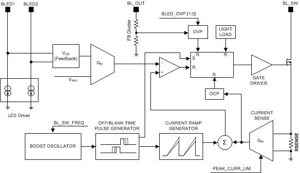 Figure 28. Backlight Boost Block Diagram
7.3.1.9.1 Headroom Voltage
In order to optimize efficiency, the LED driver-regulated headroom voltage (VHR) changes with the programmed LED current. This allows for increased solution efficiency as the dropout voltage of the LED driver changes. Furthermore, in order to ensure that both current sinks remain in regulation when there is a mismatch in string voltages, the minimum headroom voltage between VBLED1 and VBLED2 becomes the regulation point for the boost converter. For example, if the LEDs connected to BLED1 require 25 V at the programmed current, and the LEDs connected to BLED2 require 25.5 V at the programmed current, the voltage at BLED1 is VHR + 0.5 V, and the voltage at BLED2 is VHR. In other words, the cathode of the highest voltage LED string becomes the boost output regulation point.
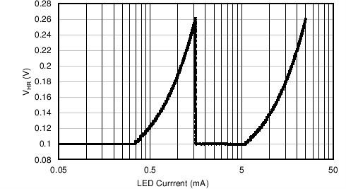 Figure 29. Regulated Headroom vs LED Current
7.3.1.9.2 Backlight Protection and Faults
7.3.1.9.2.1 Overvoltage Protection (OVP) and Open-Load Fault Protection
The LM3632A provides an OVP that monitors the LED boost output voltage (VBL_OUT) and protects BL_OUT and BL_SW from exceeding safe operating voltages. The OVP threshold can be set to 18 V, 22 V, 25 V or 29 V with register 0x02 bits[7:5]. Once an OVP event has been detected, the BL_OVP flag is set in the Flags1 register, and the subsequent behavior depends on the state of bit BL_OVP_SET in the Enable Register: If BL_OVP_SET is set to '0', as soon as VBL_OUT falls below the backlight OVP threshold, the LM3632A begins switching again. If BL_OVP_SET is set to '1' and the device detects three occurrences of VBL_OUT > VOVP_BL while any of the enabled current sink headroom voltages drops below 40 mV, the BL_OVP flag is set, the Backlight Enable bit is cleared, and the LM3632A enters standby mode. When the device is shut down due to a BL_OVP fault the Flags1 register must be read back before the device can be reenabled.
7.3.1.9.2.2 Overcurrent Protection (OCP) and Overcurrent Protection Flag
The LM3632A has an OCP threshold of 1 A. The OCP threshold is a cycle-by-cycle current limit detected in the low-side NFET. Once the threshold is reached, the NFET turns off for the remainder of the switching period. If enough overcurrent events occur, the BL_OCP flag (register 0x10 bit[0]) is set. The flag can be cleared upon a readback of register 0x10. To avoid transient conditions from inadvertently setting the BL_OCP flag, a pulse density counter monitors BL_OCP events over a 128-µs time window. If 8 consecutive 128-µs windows of at least 2 OCP events are detected, the BL_OCP flag is set.
7.3.2 LCM Bias
7.3.2.1 Display Bias Boost Converter (VVPOS, VVNEG)
A single high-efficiency boost converter provides a positive voltage rail, VLCM_OUT, which serves as the power rail for the LCM VPOS and VNEG outputs.
- The VVPOS output LDO has a programmable range from 4 V up to 6 V with 50-mV steps and can supply up to 50 mA.
- The VVNEG output is generated from a regulated, inverting charge pump and has an adjustable range of –6 V up to –4 V with 50-mV steps and a maximum load of 50 mA.
Boost voltage also has a programmable range from 4.5 V up to 6.4 V with 50-mV steps. Please refer to Table 19, Table 20 and Table 21 for VLCM_OUT, VVPOS and VVNEG voltage settings. When selecting a suitable boost-output voltage, the following estimation can be used: VLCM_OUT = max(VVPOS, |VVNEG|) + VHR, where VHR = 300 mV for lower currents and 400 mV for higher currents. When the device input voltage (VIN) is greater than the programmed LCM boost output voltage, the boost voltage goes to VIN + 100 mV. VVPOS, and VVNEG voltage settings cannot be changed while they are enabled. While the VLCM_OUT target changes immediately upon a register write, VVPOS and VVNEG register setting targets take effect only after the outputs are disabled and re-enabled.
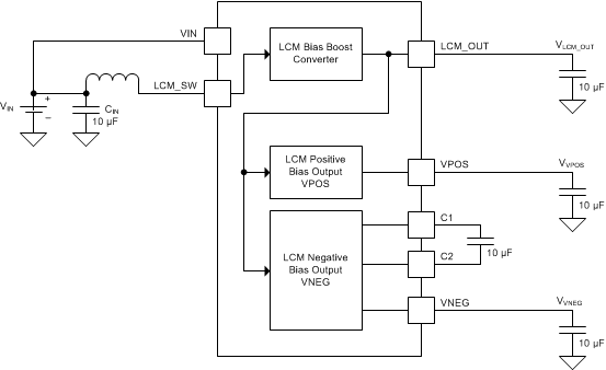 Figure 30. LCM Boost Block Diagram
The LCM Bias outputs can be controlled either by pins LCM_EN1 and LCM_EN2 or register bits VPOS_EN and VNEG_EN, register 0x0C bits[2:1]. Setting bit EXT_EN, register 0x0C bit[0], to '0' allows pins LCM_EN1 and LCM_EN2 to control VPOS and VNEG, respectively, while setting this bit to '1' yields control to bits VPOS_EN and VNEG_EN. Refer to Table 3 for LCM bias control information.
Table 3. LCM Bias Truth Table
| EN PIN | LCM_EN2 PIN |
LCM_EN1 PIN |
EXT_EN 0x0C[0] |
VNEG_EN 0x0C[1] |
VPOS_EN 0x0C[2] |
AUTO_SEQ 0x0C[5] |
WAKE-UP 0x0C[7] |
ACTION |
|---|---|---|---|---|---|---|---|---|
| 0 | X | X | X | X | X | X | X | Shutdown |
| 1 | 0 | 0 | 1 | X | X | X | 0 | Standby |
| 1 | 0 | 1 | 1 | X | X | X | 0 | External VPOS |
| 1 | 1 | 0 | 1 | X | X | X | 0 | External VNEG |
| 1 | 1 | 1 | 1 | X | X | 0 | 0 | External VPOS and VNEG Independent |
| 1 | 1 | 1 | 1 | X | X | 1 | 0 | External VPOS and VNEG Auto Sequence |
| 1 | X | X | 0 | 0 | 0 | X | 0 | Standby |
| 1 | X | X | 0 | 0 | 1 | X | 0 | I2C VPOS |
| 1 | X | X | 0 | 1 | 0 | X | 0 | I2C VNEG |
| 1 | X | X | 0 | 1 | 1 | 0 | 0 | I2C VPOS and VNEG Independent |
| 1 | X | X | 0 | 1 | 1 | 1 | 0 | I2C VPOS and VNEG Auto Sequence |
| 1 | 0 | X | X | X | X | X | 1 | Standby |
| 1 | 1 | X | X | 0 | 0 | X | 1 | Standby |
| 1 | 1 | X | X | 0 | 1 | X | 1 | Wake-up VPOS |
| 1 | 1 | X | X | 1 | 0 | X | 1 | Wake-up VNEG |
| 1 | 1 | X | X | 1 | 1 | X | 1 | Wake-up VPOS and VNEG |
7.3.2.2 Auto Sequence Mode
If this mode is selected the LM3632A controls the turn-on and turn-off of VPOS and VNEG as shown in Figure 31.
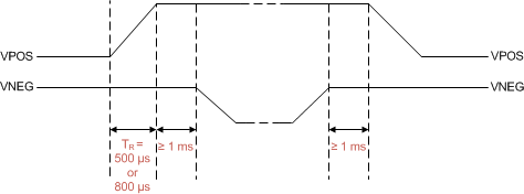 Figure 31. Auto Sequence Timing
7.3.2.3 Wake-up Mode
If Wake-up mode is selected the LM3632A allows on/off control of both VPOS and VNEG with only one external pin (LCM_EN2). Any combination of VPOS, VNEG, or both can be turned on based on the state of bits VPOS_EN and VNEG_EN in register 0x0C. In this mode the internal shutdown timing of the VPOS and VNEG blocks is modified to allow for lower quiescent current in standby mode, therefore reducing the average current consumption during a sequence of on/off events.
7.3.2.4 Active Discharge
An optional active discharge is available for the VPOS and VNEG output rails. An internal switch resistance for this discharge function is implemented on each output rail. The VPOS active discharge function is enabled with register 0x0C bit[4] and the VNEG active discharge with register 0x0C bit[3].
NOTE
To avoid an unsafe operating condition when the active discharge function is enabled, a minimum delay of 1 millisecond needs to be maintained between disabling and re-enabling of the VNEG output.
7.3.2.5 LCM Bias Protection and Faults
The LCM Bias block of the LM3632A provides four protection mechanisms in order to prevent damage to the device. Note that none of these have any effect on backlight or flash operation.
7.3.2.5.1 LCM Overvoltage Protection
The LM3632A provides OVP that monitors the LCM Bias boost output voltage (VLCM_OUT) and protects LCM_OUT and LCM_SW from exceeding safe operating voltages. The OVP threshold is set to 7 V (typical). If an LCM Bias overvoltage condition is detected, the LCM_OVP flag, register 0x10 bit[5], is set. The flag can be cleared with an I2C read back of the register. An LCM OVP condition will not cause the LCM Bias to shut down; it is a report-only flag.
7.3.2.5.2 VNEG Overvoltage Protection
If the charge-pump voltage goes 250 mV (typical) below its target set-point, the LM3632A provides a mechanism for preventing the voltage from increasing even further and damaging the device and sets the VNEG_OVP flag, register 0x10 bit[4]. The flag can be cleared with an I2C readback of the register. A VNEG OVP condition will not cause the charge pump to shut down; it is a report-only flag.
NOTE
The VNEG_OVP flag may get set during VNEG start-up under light load and low VNEG voltage settings due to VNEG voltage undershoot. After the flag is cleared via register read back, the LM3632A detects VNEG OVP conditions properly.
7.3.2.5.3 VPOS Short Circuit Protection
If the current at VPOS exceeds 80 mA (typical), the LM3632A sets the VPOS_SHORT flag, register 0x10 bit[3]. A readback of register 0x10 is required to clear the flag. A VPOS_SHORT condition will not cause the LCM Bias to shut down; it is a report-only flag.
7.3.2.5.4 VNEG Short Circuit Protection
If the voltage at VNEG goes within 750 mV (typical) from ground, the LM3632A sets the VNEG_SHORT flag, register 0x10 bit[2]. A readback of register 0x10 is required to clear the flag. A VNEG_SHORT condition will not cause the LCM Bias to shut down; it is a report-only flag.
7.3.3 Flash
7.3.3.1 Flash Boost Converter
The LM3632A incorporates a high-efficiency synchronous current-mode PWM boost converter that switches and boosts the output to maintain at least VHR across the flash current source (FLED) over the 2.7-V to 5.5-V input voltage range. The flash boost has two switching frequency modes, 2-MHz and 4-MHz. These are set via the FL_FREQ Select bits, register 0x07 bits[7:6].
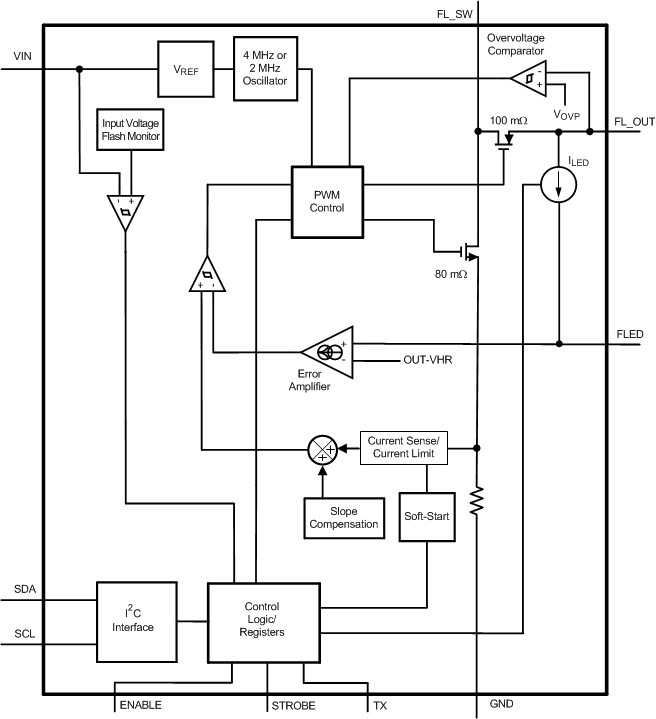 Figure 32. Flash Boost Block Diagram
7.3.3.2 Start-Up (Enabling The Device)
The flash LED output (FLED) can be enabled in flash or torch mode with the Enable Register and the STROBE pin. The state of bit STROBE_EN, register 0x09 bit[4], determines if the FLED output is enabled by bit[1] of register 0x0A or the STROBE pin. Table 4 contains the details for flash operation control. While a positive edge is required at the STROBE pin in order to initiate a Torch or Flash event, the STROBE pin is level sensitive. That means that the event is terminated as soon as the STROBE pin transitions low.
Table 4. Flash Truth Table
| EN PIN | STROBE_EN 0x09[4] |
STROBE PIN |
FLASH_EN 0x0A[1] |
FLASH_MODE 0x0A[2] |
ACTION |
|---|---|---|---|---|---|
| 0 | X | X | X | X | Shutdown |
| 1 | 0 | X | 0 | X | Standby |
| 1 | 0 | X | 1 | 0 | Int Torch |
| 1 | 0 | X | 1 | 1 | Int Flash |
| 1 | 1 | 0 | 0 | X | Standby |
| 1 | 1 | 0 | 1 | X | Standby |
| 1 | 1 | pos edge | 0 | X | Standby |
| 1 | 1 | pos edge | 1 | 0 | Ext Torch |
| 1 | 1 | pos edge | 1 | 1 | Ext Flash |
On start-up, when VOUT is less than VIN the internal synchronous PFET turns on as a current source and delivers 200 mA (typical) to the output capacitor. During this time the current source (LED) is off. When the voltage across the output capacitor reaches 2.2 V (typical) the current source turns on. At turn-on the current source steps through each flash or torch level until the target LED current is reached. This gives the device a controlled turn-on and limits inrush current from the VIN supply.
7.3.3.3 Pass Mode
The LM3632A flash boost starts up in pass mode and stays there until boost mode is needed to maintain regulation. If the voltage difference between VFL_OUT and VFLED falls below VHR, the device switches to boost mode. In pass mode the boost converter does not switch, and the synchronous PFET turns fully on bringing VFL_OUT up to VIN − IFLED × RPMOS. In pass mode the inductor current is not limited by the peak current limit.
7.3.3.4 Flash Mode
In flash mode, the LED current source (FLED) provides 15 target current levels from 100 mA to 1500 mA in 100 mA increments. The flash currents are adjusted via register 0x06 (see Table 12 for details). Once the flash sequence is activated the current source (FLED) ramps up to the programmed flash current by stepping through all current steps until the programmed current is reached. The headroom in the current source is regulated to provide 100 mA to 1.5 A to the output. Whether the device is enabled in flash mode through the Enable Register or through the STROBE pin, the Flash Enable bit in the Enable Register is cleared at the completion of the flash event and needs to be re-written in order to perform the next internal or external flash event.
7.3.3.5 Torch Mode
In torch mode, the LED current source (FLED) provides 15 target current levels from 25 mA to 375 mA in 25-mA increments. The torch currents are adjusted via register 0x06 (see Table 12 for details). Once the torch sequence is activated the current source (FLED) ramps up to the programmed Torch current by stepping through all current steps until the programmed current is reached. Torch mode is not affected by Flash Timeout or by a TX Interrupt event.
7.3.3.6 Power Amplifier Synchronization (TX)
The TX pin is a Power Amplifier Synchronization input. This is designed to reduce the flash FLED current and thus limit the battery current during high battery-current conditions such as PA transmit events. When the LM3632A is engaged in a flash event, and the TX pin is pulled high, the FLED current is forced into torch mode at the programmed torch current setting. If the TX pin is then pulled low before the flash pulse terminates, the FLED current returns to the previous flash current level. At the end of the flash time-out, whether the TX pin is high or low, the FLED current is turned off.
7.3.3.7 VIN Monitor
The LM3632A has the ability to adjust the flash current based upon the voltage level present at the VIN pin. The adjustable VINM threshold ranges from 2.6 V to 3.3 V in 100-mV steps. The Flags1 Register (0x0B) has the fault flag set when the input voltage crosses the VINM value. Additionally, the VINM threshold sets the input voltage boundary that forces the device to either transition into torch mode at the programmed torch current setting or turn off the FLED current for the remaining flash duration. This decision is made based on the status of bit VINM_MODE, register 0x09 bit[1]. In order to re-enable the LM3632A in torch or flash mode the VINM flag has to be cleared. If the VINM flag is tripped during flash current ramp-up, and VINM mode is set to torch, the FLED current is reduced not to the torch current setting but to the same percentage of the last flash current that was reached during fash current ramp-up. For example, if the flash current setting is 1 A, the torch current setting is 100 mA and the maximum flash current that was reached before the VINM threshold was crossed is 700 mA, the device will transition the flash current to 70 mA (70% of 100 mA).
7.3.3.8 Flash Fault Protections
7.3.3.8.1 Fault Operation
If the LM3632A enters a fault condition during flash, the device sets the appropriate flag in the Flags1 and Flags2 Registers (0x0B and 0x10) and places the flash block into standby by clearing the FLASH_EN bit in the Enable Register. The flash block remains in shutdown until an I2C read of the Flag Registers is completed. Upon clearing the flags/faults, flash can be restarted. If the fault is still present, the LM3632A re-enters the fault state and enters standby again. Flash faults have no effect on Backlight or LCM control.
7.3.3.8.2 Flash Time-Out
The Flash Time-Out period sets the amount of time that the Flash Current is being sourced from the current source (FLED). The LM3632A has 32 timeout levels ranging from 32 ms to 1024 ms (see Table 13 for more detail). Once a flash event is completed, the FTO flag in Flags1 register (register 0x0B bit[1]) is set. If a flash event is activated via the STROBE pin and STROBE transitions low after the end of the programmed flash timeout, the flash event is terminated at the programmed flash timeout, and the FTO flag is set. If the STROBE pin transitions low before the end of the programmed flash timeout, the flash event is terminated, and the FTO flag is not set.
7.3.3.8.3 Overvoltage Protection (OVP)
The flash output voltage is limited to typically 4.9 V (see VOVP Spec in Electrical Characteristics). In situations such as an open FLED, the LM3632A tries to raise the output voltage in order to keep the FLED current at its target value. When VFL_OUT reaches 4.9 V (typical), the overvoltage comparator trips and turns off the internal NFET. When VFL_OUT falls below the VOVP Off threshold, the LM3632A begins switching again. The Flash Enable bit is cleared, and the FLASH_OVP flag is set, when an OVP condition is present for three rising OVP edges. This prevents momentary OVP events from forcing the device to shut down.
7.3.3.8.4 Current Limit
The LM3632A features two selectable flash inductor current limits that are programmable through the I2C-compatible interface. When the inductor current limit is reached, the device terminates the charging phase of the switching cycle. Switching resumes at the start of the next switching period. If the overcurrent condition persists, the device operates continuously in current limit. Since the current limit is sensed in the NMOS switch, there is no mechanism to limit the current when the device operates in pass mode (current does not flow through the NMOS in pass mode). In boost mode or pass mode if VFL_OUT falls below 2.3 V, the device stops switching, and the PFET operates as a current source limiting the current to 200 mA. This prevents damage to the LM3632A and excessive current draw from the battery during output short-circuit conditions. The Flash Enable bit is not cleared upon a current limit event, but the FLASH_OCP flag (register 0x10 bit[1]) is set.
7.3.3.8.5 FLED and/or FL_OUT Short Fault
The FLED short flag (FLED_SHORT) reads back a '1' if the device is active in flash or torch mode and the FLED output experiences a short condition. The flash output short flag (FOUT_SHORT) reads back a '1' if the device is active in flash or torch mode and the flash boost output experiences a short condition. A FLED short condition is determined if the voltage at FLED goes below 500 mV (typical) while the device is in torch or flash mode. There is a deglitch time of 256 μs before the LED Short flag is valid and a deglitch time of 2.048 ms before the FL_OUT Short flag is valid. The FLED Short Fault can only be reset to '0' by removing power to the LM3632A, setting EN to '0', setting the SW RESET bit to a '1', or by reading back the Flags1 Register (0x0B on device). The Flash Enable bit is cleared upon a FLED and/or FL_OUT short fault.
7.3.4 Software RESET
Bit[7] (SWR_RESET) of the Enable Register (0x0A) is a software reset bit. Writing an '1' to this bit resets all I2C register values to their default values. Once the LM3632A has finished resetting all registers, it auto-clears the SWR_RESET bit.
7.3.5 EN Input
The EN pin is a global hardware enable for the LM3632A. This pin must be pulled to logic HIGH to enable the device and the I2C-compatible interface. There is a 300-kΩ internal resistor between EN and GND. When this pin is at logic LOW, the LM3632A is placed in shutdown, the I2C-compatible interface is disabled, and the internal registers are reset to their default state. It is recommended that VIN has risen above 2.7 V before setting EN HIGH and that the EN pin is not forced low while the VNEG output is enabled or before the VNEG output is discharged.
7.3.6 Thermal Shutdown (TSD)
The LM3632A has TSD protection which shuts down the backlight boost, both backlight current sinks, LCM Bias Boost and outputs, inverting charge pump, flash boost, and flash current source when the die temperature reaches or exceeds 140°C (typical). The I2C interface remains active during a TSD event. If a TSD fault occurs the TSD fault is set, register 0x0B bit[0]. The fault is cleared by an I2C read of register 0x0B or by toggling the EN pin.
7.4 Device Functional Modes
7.4.1 Modes of Operation
-
Shutdown:
The LM3632A is in shutdown when the EN pin is low.
-
Standby:
After the EN pin is set high the LM3632A goes into standby mode. In standby mode, I2C writes are allowed but references, bias currents, the oscillator, LCM powers, backlight and flash are all disabled, to keep the quiescent supply current low (2 µA typ.).
7.5 Programming
7.5.1 I2C-Compatible Serial Bus Interface
7.5.1.1 Interface Bus Overview
The I2C-compatible synchronous serial interface provides access to the programmable functions and registers on the device. This protocol uses a two-wire interface for bidirectional communications between the IC's connected to the bus. The two interface lines are the Serial Data Line (SDA) and the Serial Clock Line (SCL). These lines should be connected to a positive supply via a pull-up resistor and remain HIGH even when the bus is idle.
Every device on the bus is assigned a unique address and acts as either a Master or a Slave, depending whether it generates or receives the serial clock (SCL).
7.5.1.2 Data Transactions
One data bit is transferred during each clock pulse. Data is sampled during the high state of the serial clock (SCL). Consequently, throughout the clock’s high period, the data should remain stable. Any changes on the SDA line during the high state of the SCL and in the middle of a transaction, aborts the current transaction. New data should be sent during the low SCL state. This protocol permits a single data line to transfer both command/control information and data using the synchronous serial clock.
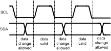 Figure 33. Data Validity
Each data transaction is composed of a Start Condition, a number of byte transfers (set by the software), and a Stop Condition to terminate the transaction. Every byte written to the SDA bus must be 8 bits long and is transferred with the most significant bit first. After each byte, an Acknowledge signal must follow. The following sections provide further details of this process.
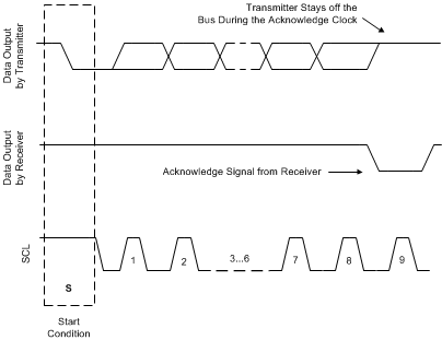 Figure 34. Acknowledge Signal
The Master device on the bus always generates the Start and Stop Conditions (control codes). After a Start Condition is generated, the bus is considered busy, and it retains this status until a certain time after a Stop Condition is generated. A high-to-low transition of the data line (SDA) while the clock (SCL) is high indicates a Start Condition. A low-to-high transition of the SDA line while the SCL is high indicates a Stop Condition.
 Figure 35. Start and Stop Conditions
In addition to the first Start Condition, a repeated Start Condition can be generated in the middle of a transaction. This allows another device to be accessed, or a register read cycle.
7.5.1.3 Acknowledge Cycle
The Acknowledge Cycle consists of two signals: the acknowledge clock pulse the master sends with each byte transferred, and the acknowledge signal sent by the receiving device.
The master generates the acknowledge clock pulse on the ninth clock pulse of the byte transfer. The transmitter releases the SDA line (permits it to go high) to allow the receiver to send the acknowledge signal. The receiver must pull down the SDA line during the acknowledge clock pulse and ensure that SDA remains low during the high period of the clock pulse, thus signaling the correct reception of the last data byte and its readiness to receive the next byte.
7.5.1.4 Acknowledge After Every Byte Rule
The master generates an acknowledge clock pulse after each byte transfer. The receiver sends an acknowledge signal after every byte received.
There is one exception to the “acknowledge after every byte” rule. When the master is the receiver, it must indicate to the transmitter an end of data by not-acknowledging (“negative acknowledge”) the last byte clocked out of the slave. This “negative acknowledge” still includes the acknowledge clock pulse (generated by the master), but the SDA line is not pulled down.
7.5.1.5 Addressing Transfer Formats
Each device on the bus has a unique slave address. The LM3632A operates as a slave device with the 7-bit address. If an 8-bit address is used for programming, the 8th bit is '1' for read and '0' for write. The 7-bit address for the device is 0x11.
Before any data is transmitted, the master transmits the address of the slave being addressed. The slave device should send an acknowledge signal on the SDA line, once it recognizes its address. The slave address is the first seven bits after a Start Condition. The direction of the data transfer (R/W) depends on the bit sent after the slave address — the eighth bit.
When the slave address is sent, each device in the system compares this slave address with its own. If there is a match, the device considers itself addressed and sends an acknowledge signal. Depending upon the state of the R/W bit (1:read, 0:write), the device acts as a transmitter or a receiver.
 Figure 36. I2C Device Address
- Master device generates start condition.
- Master device sends slave address (7 bits) and the data direction bit (r/w = 0).
- Slave device sends acknowledge signal if the slave address is correct.
- Master sends control register address (8 bits).
- Slave sends acknowledge signal.
- Master sends data byte to be written to the addressed register.
- Slave sends acknowledge signal.
- If master sends further data bytes the control register address is incremented by one after acknowledge signal.
- Write cycle ends when the master creates stop condition.
Control Register Write Cycle
- Master device generates a start condition.
- Master device sends slave address (7 bits) and the data direction bit (r/w = 0).
- Slave device sends acknowledge signal if the slave address is correct.
- Master sends control register address (8 bits).
- Slave sends acknowledge signal
- Master device generates repeated start condition.
- Master sends the slave address (7 bits) and the data direction bit (r/w = 1).
- Slave sends acknowledge signal if the slave address is correct.
- Slave sends data byte from addressed register.
- If the master device sends acknowledge signal, the control register address is incremented by one. Slave device sends data byte from addressed register.
- Read cycle ends when the master does not generate acknowledge signal after data byte and generates stop condition.
Control Register Read Cycle
Table 5. I2C Data Read/Write(1)
| ADDRESS MODE | |
|---|---|
| Data Read | <Start Condition> <Slave Address><r/w =0>[Ack] <Register Addr>[Ack] <Repeated Start Condition> <Slave Address><r/w = 1>[Ack] [Register Data]<Ack or NAck> ...additional reads from subsequent register address possible <Stop Condition> |
| Data Write | <Start Condition> <Slave Address><r/w = 0>[Ack] <Register Addr>[Ack] <Register Data>[Ack] ...additional writes to subsequent register address possible <Stop Condition> |
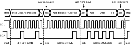 Figure 37. Register Write Format
When a READ function is to be accomplished, a WRITE function must precede the READ function, as show in the Read Cycle waveform.
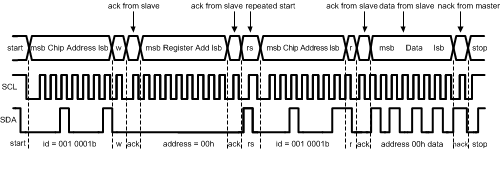 Figure 38. Register Read Format
NOTE
w = write (SDA = 0), r = read (SDA = 1), ack = acknowledge (SDA pulled down by either master or slave), rs = repeated start id = 7-bit chip address
7.6 Register Maps
Table 6. Register Default Values
| I2C Address | Register Name | Read/Write | Power On/Reset Value |
|---|---|---|---|
| 0x01 | Revision Register | R | 0x09 |
| 0x02 | Backlight Configuration1 Register | R/W | 0x30 |
| 0x03 | Backlight Configuration2 Register | R/W | 0x0D |
| 0x04 | LED Brightness LSB Register | R/W | 0x07 |
| 0x05 | LED Brightness MSB Register | R/W | 0xFF |
| 0x06 | Flash/Torch Current Register | R/W | 0x3E |
| 0x07 | Flash Configuration Register | R/W | 0x2F |
| 0x08 | VIN Monitor Register | R/W | 0x03 |
| 0x09 | I/O Control Register | R/W | 0x00 |
| 0x0A | Enable Register | R/W | 0x00 |
| 0x0B | Flags1 Register | R | 0x00 |
| 0x0C | Display Bias Configuration Register | R/W | 0x18 |
| 0x0D | LCM Boost Bias Register | R/W | 0x1E |
| 0x0E | VPOS Bias Register | R/W | 0x1E |
| 0x0F | VNEG Bias Register | R/W | 0x1C |
| 0x10 | Flags2 Register | R | 0x00 |
7.6.1 Revision (Address = 0x01) [reset = 0x09]
| 7 | 6 | 5 | 4 | 3 | 2 | 1 | 0 |
| DEV_REV[5] | DEV_REV[4] | DEV_REV[3] | DEV_REV[2] | DEV_REV[1] | DEV_REV[0] | VENDOR[1] | VENDOR[0] |
| R-0 | R-0 | R-0 | R-0 | R-1 | R-0 | R-0 | R-1 |
| LEGEND: R/W = Read/Write; R = Read only; -n = value after reset |
Table 7. Revision Register Field Descriptions
| Bit | Field | Type | Reset | Description |
|---|---|---|---|---|
| 7-2 | DEV_REV[6:0] | R | 000010 | |
| 1-0 | VENDOR[1:0] | R | 01 |
7.6.2 Backlight Configuration1 (Address = 0x02) [reset = 0x30]
| 7 | 6 | 5 | 4 | 3 | 2 | 1 | 0 |
| BLED_OVP[2] | BLED_OVP[1] | BLED_OVP[0] | BLED_MAP | PWM_CONFIG | Reserved | ||
| R/W-0 | R/W-0 | R/W-1 | R/W-1 | R/W-0 | |||
| LEGEND: R/W = Read/Write; R = Read only; -n = value after reset |
Table 8. Backlight Configuration1 Register Field Descriptions
| Bit | Field | Type | Reset | Description |
|---|---|---|---|---|
| 7-5 | BLED_OVP | R/W | 001 | Backlight OVP level select 000: 18 V 001: 22 V (Default) 010: 25 V 011: 29 V Note: Codes 100 to 111 also map to 29 V |
| 4 | BLED_MAP | R/W | 1 | Sets the backlight LED mapping mode 0: Exponential 1: Linear (Default) |
| 3 | PWM_CONFIG | R/W | 0 | Sets the polarity of the PWM input signal 0: Active High PWM Input (default) 1: Active Low PWM Input |
| 2-0 | Reserved |
7.6.3 Backlight Configuration2 (Address = 0x03) [reset = 0x0D]
| 7 | 6 | 5 | 4 | 3 | 2 | 1 | 0 |
| BL_FREQ | BL_TRANS[3] | BL_TRANS[2] | BL_TRANS[1] | BL_TRANS[0] | PWM_FREQ | PWM_HYST[1] | PWM_HYST[0] |
| R/W-0 | R/W-0 | R/W-0 | R/W-0 | R/W-1 | R/W-1 | R/W-0 | R/W-1 |
| LEGEND: R/W = Read/Write; R = Read only; -n = value after reset |
Table 9. Backlight Configuration2 Register Field Descriptions
| Bit | Field | Type | Reset | Description |
|---|---|---|---|---|
| 7 | BL_FREQ | R/W | 0 | Sets the backlight boost switch frequency 0: 500 kHz (Default)
|
| 6-3 | BL_TRANS[3:0] | R/W | 001 | Controls backlight LED ramping time. The transient time is a constant time that the backlight takes to transition from an existing programmed code to a new programmed code. 0000: 0 0001: 500 µs (Default) 0010: 750 µs 0011: 1 ms 0100: 2 ms 0101: 5 ms 0110: 10 ms 0111: 20 ms 1000: 50 ms 1001: 100 ms 1010: 250 ms 1011: 800 ms 1100: 1 s 1101: 2 s 1110: 4 s 1111: 8 s |
| 2 | PWM_FREQ | R/W | 1 | Sets PWM sampling frequency 0: 1 MHz 1: 4 MHz (Default) |
| 1-0 | PWM_HYST[1:0] | R/W | 01 | Sets the minimum change in PWM input duty cycle that results in a change of backlight LED brightness level 00: 1 bit 01: 2 bits (Default) 10: 4 bits 11: 6 bits |
7.6.4 Backlight Brightness LSB (Address = 0x04) [reset = 0x07]
| 7 | 6 | 5 | 4 | 3 | 2 | 1 | 0 |
| Reserved | BL_BRT_ LSB[2] |
BL_BRT_ LSB[1] |
BL_BRT_ LSB[0] |
||||
| R/W-1 | R/W-1 | R/W-1 | |||||
| LEGEND: R/W = Read/Write; R = Read only; -n = value after reset |
Table 10. Backlight Brightness LSB Register Field Descriptions
| Bit | Field | Type | Reset | Description |
|---|---|---|---|---|
| 7-3 | Reserved | |||
| 2-0 | BL_BRT_LSB[2:0] | R/W | 111 | Lower 3 bits (LSB's) of brightness code. Concatenated with brightness bits in Register 0x05 (MSB). |
7.6.5 Backlight Brightness MSB (Address = 0x05) [reset = 0xFF]
| 7 | 6 | 5 | 4 | 3 | 2 | 1 | 0 |
| BL_BRT_ MSB[7] |
BL_BRT_ MSB[6] |
BL_BRT_ MSB[5] |
BL_BRT_ MSB[4] |
BL_BRT_ MSB[3] |
BL_BRT_ MSB[2] |
BL_BRT_ MSB[1] |
BL_BRT_ MSB[0] |
| R/W-1 | R/W-1 | R/W-1 | R/W-1 | R/W-1 | R/W-1 | R/W-1 | R/W-1 |
| LEGEND: R/W = Read/Write; R = Read only; -n = value after reset |
Table 11. Backlight Brightness MSB Register Field Descriptions
| Bit | Field | Type | Reset | Description |
|---|---|---|---|---|
| 7-0 | BL_BRT_MSB[7:0] | R/W | 11111111 | Upper 8 bits (MSB's) of backlight brightness code. Concatenated with brightness bits in Register 0x04 (LSB). With linear mapping the 11-bit code to current response is approximated by the equation: ILED=37.8055μA+12.1945μA×I2C_BRGT_CODE (for codes > 0). With exponential mapping the 11-bit code-to-current response is approximated by the equation: ILED=50μA×1.003040572I2C_BRGT_CODE (for codes > 0). These equations are valid for I2C brightness codes between 1 and 2047. Code 0 disables the backlight. |
7.6.6 Flash/Torch Current (Address = 0x06) [reset = 0x3E]
| 7 | 6 | 5 | 4 | 3 | 2 | 1 | 0 |
| TORCH_ BRT[3] |
TORCH_ BRT[2] |
TORCH_ BRT[1] |
TORCH_ BRT[0] |
FLASH_ BRT[3] |
FLASH_ BRT[2] |
FLASH_ BRT[1] |
FLASH_ BRT[0] |
| R/W-0 | R/W-0 | R/W-1 | R/W-1 | R/W-1 | R/W-1 | R/W-1 | R/W-0 |
| LEGEND: R/W = Read/Write; R = Read only; -n = value after reset |
Table 12. Flash/Torch Current Register Field Descriptions
| Bit | Field | Type | Reset | Description |
|---|---|---|---|---|
| 7-4 | TORCH_BRT[3:0] | R/W | 0011 | Sets torch mode current level (25 mA per step) 0000: 25 mA 0001: 50 mA 0010: 75 mA 0011: 100 mA (Default) .................... 1101: 350 mA 1110: 375 mA Note: Code 1111 also maps to 375 mA |
| 3-0 | FLASH_BRT[3:0] | R/W | 1110 | Sets flash mode current level (100 mA per step) 0000: 100 mA 0001: 200 mA 0010: 300 mA 0011: 400 mA .................... 1101: 1.4 A 1110: 1.5 A (Default) Note: Code 1111 also maps to 1.5 A |
7.6.7 Flash Configuration (Address = 0x07) [reset = 0x2F]
| 7 | 6 | 5 | 4 | 3 | 2 | 1 | 0 |
| FL_FREQ[1] | FL_FREQ[0] | FL_ILIMIT | FTO[4] | FTO[3] | FTO[2] | FTO[1] | FTO[0] |
| R/W-0 | R/W-0 | R/W-1 | R/W-0 | R/W-1 | R/W-1 | R/W-1 | R/W-1 |
| LEGEND: R/W = Read/Write; R = Read only; -n = value after reset |
Table 13. Flash Configuration Register Field Descriptions
| Bit | Field | Type | Reset | Description |
|---|---|---|---|---|
| 7-6 | FL_FREQ[1:0] | R/W | 00 | Sets the flash boost switch frequency 00: 4 MHz (Default) 01: 2 MHz Note: Codes 10 and 11 also map to 2 MHz |
| 5 | FL_ILIMIT | R/W | 1 | Selects the switch current limit level for flash boost 0: 1.9 A 1: 2.8 A (Default) |
| 4-0 | FTO[4:0] | R/W | 01111 | Selects the flash timeout duration (32 ms per step) 00000: 32 ms 00001: 64 ms 00010: 96 ms 00011: 128 ms ..................... 01110: 480 ms 01111: 512 ms (Default) 10000: 544 ms ..................... 11110: 992 ms 11111: 1024 ms |
7.6.8 VIN Monitor (Address = 0x08) [reset = 0x03]
| 7 | 6 | 5 | 4 | 3 | 2 | 1 | 0 |
| Reserved | VINM[2] | VINM[1] | VINM[0] | ||||
| R/W-0 | R/W-1 | R/W-1 | |||||
| LEGEND: R/W = Read/Write; R = Read only; -n = value after reset |
Table 14. VIN Monitor Register Field Descriptions
| Bit | Field | Type | Reset | Description |
|---|---|---|---|---|
| 7-3 | Reserved | |||
| 2-0 | VINM[2:0] | R/W | 011 | This field sets the VIN Monitor threshold level 000: 2.6 V 001: 2.7 V 010: 2.8 V 011: 2.9 V (Default) 100: 3 V 101: 3.1 V 110: 3.2 V 111: 3.3 V |
7.6.9 I/O Control (Address = 0x09) [reset = 0x00]
| 7 | 6 | 5 | 4 | 3 | 2 | 1 | 0 |
| Reserved | PWM_EN | Reserved | STROBE_EN | Reserved | TX_EN | VINM_MODE | VINM_EN |
| R/W-0 | R/W-0 | R/W-0 | R/W-0 | R/W-0 |
| LEGEND: R/W = Read/Write; R = Read only; -n = value after reset |
Table 15. I/O Control Register Field Descriptions
| Bit | Field | Type | Reset | Description |
|---|---|---|---|---|
| 7 | Reserved | |||
| 6 | PWM_EN | R/W | 0 | This bit enables and disables the PWM input pin. If enabled, the backlight LED current ramps up to Target_Current*PWM_Duty_Cycle. If disabled, the PWM input is ignored. 0: PWM disabled (Default) 1: PWM enabled |
| 5 | Reserved | |||
| 4 | STROBE_EN | R/W | 0 | Hardware flash enable 0: STROBE disabled (Default) 1: STROBE enabled |
| 3 | Reserved | |||
| 2 | TX_EN | R/W | 0 | Flash Interrupt mode enable 0: TX disabled (Default) 1: TX enabled |
| 1 | VINM_MODE | R/W | 0 | Selects the VIN Monitor current reduction level 0: Flash driver returns to standby mode (Default) 1: Flash current reduced to programmed Torch current level |
| 0 | VINM_EN | R/W | 0 | Set this bit to enable VIN Monitor function 0: Disabled (Default) 1: Enabled |
7.6.10 Enable (Address = 0x0A) [reset = 0x00]
| 7 | 6 | 5 | 4 | 3 | 2 | 1 | 0 |
| SWR_RESET | Reserved | BL_OVP_SET | BLED1_EN | BLED1/2_EN | FLASH_MODE | FLASH_EN | BL_EN |
| R/W-0 | R/W-0 | R/W-0 | R/W-0 | R/W-0 | R/W-0 | R/W-0 |
| LEGEND: R/W = Read/Write; R = Read only; -n = value after reset |
Table 16. Enable Register Field Descriptions
| Bit | Field | Type | Reset | Description |
|---|---|---|---|---|
| 7 | SWR_RESET | R/W | 0 | Setting this bit resets all registers to their default values. Bit auto-clears (returns to "0" upon device reset). |
| 6 | Reserved | R/W | 0 | |
| 5 | BL_OVP_SET | R/W | 0 | 0: Reports flag if OVP condition detected, but no action taken (Default) 1: OVP causes shutdown |
| 4 | BLED1_EN | R/W | 0 | Backlight sink 1 enable only 0: Disabled (Default) 1: Enabled |
| 3 | BLED1/2_EN | R/W | 0 | Backlight sink 1 and sink 2 enable. Has priority over bit[4] (BLED1_EN). 0: Backlight sink 2 disabled, backlight sink 1 status depends on BLED1_EN bit status (Default) 1: Backlight sink 1 and sink 2 enabled regardless of BLED1_EN bit status |
| 2 | FLASH_MODE | R/W | 0 | Selects Torch or Flash mode for flash LED output 0: Torch (Default) 1: Flash |
| 1 | FLASH_EN | R/W | 0 | Flash LED output enable 0: Disabled (Default) 1: Enabled |
| 0 | BL_EN | R/W | 0 | Backlight output enable 0: Disabled (Default) 1: Enabled |
7.6.11 Flags1 (Address = 0x0B) [reset = 0x00]
| 7 | 6 | 5 | 4 | 3 | 2 | 1 | 0 |
| BL_OVP | FLASH_OVP | FOUT_SHORT | VINM | TX | FLED_SHORT | FTO | TSD |
| R-0 | R-0 | R-0 | R-0 | R-0 | R-0 | R-0 | R-0 |
| LEGEND: R/W = Read/Write; R = Read only; -n = value after reset |
Table 17. Flags1 Register Field Descriptions
| Bit | Field | Type | Reset | Description |
|---|---|---|---|---|
| 7 | BL_OVP | R | 0 | Backlight overvoltage protection fault or flag |
| 6 | FLASH_OVP | R | 0 | Flash overvoltage protection fault or flag |
| 5 | FOUT_SHORT | R | 0 | Flash output short fault |
| 4 | VINM | R | 0 | VINM fault or flag |
| 3 | TX | R | 0 | TX Interrupt flag |
| 2 | FLED_SHORT | R | 0 | Flash LED short fault |
| 1 | FTO | R | 0 | Flash timeout flag |
| 0 | TSD | R | 0 | Thermal shutdown fault |
7.6.12 Display Bias Configuration (Address = 0x0C) [reset = 0x18]
| 7 | 6 | 5 | 4 | 3 | 2 | 1 | 0 |
| WAKE-UP | VPOS_TRANS | AUTOSEQ | VPOS_DISCH | VNEG_DISCH | VPOS_EN | VNEG_EN | EXT_EN |
| R/W-1 | R/W-1 | R/W-0 | R/W-0 | R/W-0 |
| LEGEND: R/W = Read/Write; R = Read only; -n = value after reset |
Table 18. Display Bias Configuration Register Field Descriptions
| Bit | Field | Type | Reset | Description |
|---|---|---|---|---|
| 7 | WAKE-UP | R/W | 0 | Enables wake-up mode 0: Wake-up mode disabled (Default) 1: Wake-up mode enabled |
| 6 | VPOS_TRANS | R/W | 0 | Controls positive display bias voltage (LDO) ramping time 0: 800 µs (Default) 1: 500 µs |
| 5 | AUTOSEQ | R/W | 0 | Enables Auto-sequence 0: Auto-sequence disabled (Default) 1: Auto-sequence enabled |
| 4 | VPOS_DISCH | R/W | 1 | Positive display bias voltage (LDO) active discharge selection 0: Not discharged 1: Active discharge (Default) |
| 3 | VNEG_DISCH | R/W | 1 | Negative display bias voltage (inverting charge pump) active discharge selection 0: Not discharged 1: Active discharge (Default) |
| 2 | VPOS_EN | R/W | 0 | Positive display bias (LDO) enable 0: Disabled (Default) 1: Enabled |
| 1 | VNEG_EN | R/W | 0 | Negative display bias (inverting charge pump) enable 0: Disabled (Default) 1: Enabled |
| 0 | EXT_EN | R/W | 0 | Setting this bit activates pins LCM_EN1 and LCM_EN2 to enable VPOS and VNEG, respectively 0: VPOS and VNEG can only be enabled via bit VPOS_EN and VNEG_EN, respectively (Default) 1: VPOS and VNEG can only be enabled via pin LCM_EN1 and LCM_EN2, respectively |
7.6.13 LCM Boost Bias (Address = 0x0D) [reset = 0x1E]
| 7 | 6 | 5 | 4 | 3 | 2 | 1 | 0 |
| Reserved | LCM_VBST[5] | LCM_VBST[4] | LCM_VBST[3] | LCM_VBST[2] | LCM_VBST[1] | LCM_VBST[0] | |
| R/W-0 | R/W-1 | R/W-1 | R/W-1 | R/W-1 | R/W-0 | ||
| LEGEND: R/W = Read/Write; R = Read only; -n = value after reset |
Table 19. LCM Boost Bias Register Field Descriptions
| Bit | Field | Type | Reset | Description |
|---|---|---|---|---|
| 7-6 | Reserved | |||
| 5-0 | LCM_VBST[5:0] | R/W | 011110 | Sets the LCM Boost Voltage (50 mV per step) 000000: 4.5 V 000001: 4.55 V 000010: 4.6 V .................... 011101: 5.95 V 011110: 6 V (Default) 011111: 6.05 V .................... 100101: 6.35 V 100110: 6.4 V Note: Codes 100111 to 111111 map to 6.4V |
7.6.14 VPOS Bias (Address = 0x0E) [reset = 0x1E]
| 7 | 6 | 5 | 4 | 3 | 2 | 1 | 0 |
| Reserved | VPOS[5] | VPOS[4] | VPOS[3] | VPOS[2] | VPOS[1] | VPOS[0] | |
| R/W-0 | R/W-1 | R/W-1 | R/W-1 | R/W-1 | R/W-0 | ||
| LEGEND: R/W = Read/Write; R = Read only; -n = value after reset |
Table 20. VPOS Bias Register Field Descriptions
| Bit | Field | Type | Reset | Description |
|---|---|---|---|---|
| 7-6 | Reserved | |||
| 5-0 | VPOS[5:0] | R/W | 011110 | Sets the Positive Display Bias (LDO) Voltage (50 mV per step) 000000: 4 V 000001: 4.05 V 000010: 4.1 V .................... 011101: 5.45 V 011110: 5.5 V (Default) 011111: 5.55 V .................... 100111: 5.95 V 101000: 6 V Note: Codes 101001 to 111111 map to 6 V |
7.6.15 VNEG Bias (Address = 0x0F) [reset = 0x1C]
| 7 | 6 | 5 | 4 | 3 | 2 | 1 | 0 |
| Reserved | VNEG[5] | VNEG[4] | VNEG[3] | VNEG[2] | VNEG[1] | VNEG[0] | |
| R/W-0 | R/W-1 | R/W-1 | R/W-1 | R/W-0 | R/W-0 | ||
| LEGEND: R/W = Read/Write; R = Read only; -n = value after reset |
Table 21. VNEG Bias Register Field Descriptions
| Bit | Field | Type | Reset | Description |
|---|---|---|---|---|
| 7-6 | Reserved | |||
| 5-0 | VNEG[5:0] | R/W | 011100 | Sets the Negative Display Bias (inverting charge pump) Voltage (–50 mV per step) 000000: –4 V 000001: –4.05 V 000010: -4.1 V .................... 011011: –5.35 V 011100: –5.4 V (Default) 011101: –5.45 V .................... 100111: –5.95 V 101000: –6 V Note: Codes 101001 to 111111 map to –6 V |
7.6.16 Flags2 (Address = 0x10) [reset = 0x00]
| 7 | 6 | 5 | 4 | 3 | 2 | 1 | 0 |
| Reserved | LCM_OVP | VNEG_OVP | VPOS_SHORT | VNEG_SHORT | FLASH_OCP | BL_OCP | |
| R-0 | R-0 | R-0 | R-0 | R-0 | R-0 | ||
| LEGEND: R/W = Read/Write; R = Read only; -n = value after reset |
Table 22. Flags2 Register Field Descriptions
| Bit | Field | Type | Reset | Description |
|---|---|---|---|---|
| 7-6 | Reserved | |||
| 5 | LCM_OVP | R | 0 | LCM boost overvoltage protection flag |
| 4 | VNEG_OVP | R | 0 | VNEG overvoltage protection flag |
| 3 | VPOS_SHORT | R | 0 | VPOS short circuit protection flag |
| 2 | VNEG_SHORT | R | 0 | VNEG short circuit protection flag |
| 1 | FLASH_OCP | R | 0 | Flash boost output overcurrent protection flag |
| 0 | BL_OCP | R | 0 | Backlight boost overcurrent protection flag |