-
LM397 Single General-Purpose Voltage Comparator
- 1 Features
- 2 Applications
- 3 Description
- 4 Revision History
- 5 Pin Configuration and Functions
- 6 Specifications
- 7 Detailed Description
- 8 Application and Implementation
- 9 Power Supply Recommendations
- 10Layout
- 11Device and Documentation Support
- 12Mechanical, Packaging, and Orderable Information
- IMPORTANT NOTICE
Package Options
Mechanical Data (Package|Pins)
- DBV|5
Thermal pad, mechanical data (Package|Pins)
Orderable Information
LM397 Single General-Purpose Voltage Comparator
1 Features
- TA = 25°C. Typical Values Unless Otherwise Specified.
- 5-Pin SOT-23 Package
- Industrial Operating Range −40°C to +85°C
- Single or Dual Power Supplies
- Wide Supply Voltage Range 5 V to 30 V
- Low Supply Current 300 µA
- Low Input Bias Current 7 nA
- Low Input Offset Current ±1 nA
- Low Input Offset Voltage ±2 mV
- Response Time 440 ns (50-mV Overdrive)
- Input Common-Mode Voltage 0 to VS – 1.5 V
2 Applications
- A/D Converters
- Pulse, Square-Wave Generators
- Peak Detector
- Industrial Applications
3 Description
The LM397 device is a single voltage comparator with an input common mode that includes ground. The LM397 is designed to operate from a single 5-V to 30-V power supply or a split power supply. Its low supply current is virtually independent of the magnitude of the supply voltage.
The LM397 features an open-collector output stage. This allows the connection of an external resistor at the output. The output can directly interface with TTL, CMOS and other logic levels, by tying the resistor to different voltage levels (level translator).
The LM397 is available in the space-saving 5-Pin SOT-23 package and is pin-compatible to TI’s TL331, a single differential comparator.
Device Information(1)
| PART NUMBER | PACKAGE | BODY SIZE (NOM) |
|---|---|---|
| LM397 | SOT-23 (5) | 2.90 mm × 1.60 mm |
- For all available packages, see the orderable addendum at the end of the data sheet.
Typical Circuit

4 Revision History
Changes from E Revision (October 2015) to F Revision
- Changed incorrect Pin Functions table entries. Pins 4 and 5 were swapped.Go
Changes from D Revision (March 2013) to E Revision
- Added ESD Rating table, Feature Description section, Device Functional Modes, Application and Implementation section, Power Supply Recommendations section, Layout section, Device and Documentation Support section, and Mechanical, Packaging, and Orderable Information section. Go
Changes from C Revision (March 2013) to D Revision
- Changed layout of National Data Sheet to TI formatGo
6 Specifications
6.1 Absolute Maximum Ratings
over operating free-air temperature range (unless otherwise noted)(1)(2)| MIN | MAX | UNIT | ||
|---|---|---|---|---|
| VIN differential | 30 | 30 | V | |
| Supply voltages | ±15 | 30 | V | |
| Voltage at input pins | −0.3 | 30 | V | |
| Junction temperature(3) | 150 | ºC | ||
| Soldering information | Infrared or Convection (20 sec.) | 235 | ºC | |
| Wave Soldering (10 sec.) | 260 | ºC | ||
| Storage Temperature, Tstg | −65 | 150 | ºC | |
6.2 ESD Ratings
| VALUE | UNIT | |||
|---|---|---|---|---|
| V(ESD) | Electrostatic discharge | Human body model (HBM), per ANSI/ESDA/JEDEC JS-001(1)(2) | ±2000 | V |
| Machine Model(1)(2) | ±200 | |||
6.3 Recommended Operating Conditions
| MIN | MAX | UNIT | ||
|---|---|---|---|---|
| Supply voltage, VS | 5 | 30 | V | |
| Temperature(1) | −40 | 85 | °C | |
6.4 Thermal Information
| THERMAL METRIC(1) | LM397 | UNIT | |
|---|---|---|---|
| DBV (SOT-23) | |||
| 5 PINS | |||
| RθJA | Junction-to-ambient thermal resistance(2) | 186 | °C/W |
| RθJC(top) | Junction-to-case (top) thermal resistance | 92.8 | °C/W |
| RθJB | Junction-to-board thermal resistance | 38.9 | °C/W |
| ψJT | Junction-to-top characterization parameter | 5.6 | °C/W |
| ψJB | Junction-to-board characterization parameter | 38.4 | °C/W |
6.5 Electrical Characteristics
Unless otherwise specified, all limits are ensured for TA = 25°C, VS = 5 V, V− = 0 V, VCM = V+/2 = VO.| PARAMETER | TEST CONDITIONS | MIN(2) | TYP(1) | MAX(2) | UNIT | ||
|---|---|---|---|---|---|---|---|
| VOS | Input offset voltage | VS = 5 V to 30 V, VO = 1.4 V, VCM = 0 V |
TA = 25ºC | 2 | 7 | mV | |
| At the temperature extremes | 10 | ||||||
| IOS | Input offset current | VO = 1.4 V, VCM = 0 V | TA = 25ºC | 1.6 | 50 | nA | |
| At the temperature extremes | 250 | ||||||
| IB | Input bias current | VO = 1.4 V, VCM = 0 V | TA = 25ºC | 10 | 250 | nA | |
| At the temperature extremes | 400 | ||||||
| IS | Supply current | RL = open, VS = 5 V | 0.25 | 0.7 | mA | ||
| RL = open, VS = 30 V | 0.3 | 2 | |||||
| IO | Output sink current | VIN+ = 1 V, VIN− = 0 V, VO = 1.5 V | 6 | 13 | mA | ||
| ILEAKAGE | Output leakage current | VIN+ = 1 V, VIN− = 0 V, VO = 5 V | 0.1 | nA | |||
| VIN+ = 1 V, VIN− = 0 V, VO = 30 V | 1 | µA | |||||
| VOL | Output voltage low | IO = −4 mA, VIN+ = 0 V, VIN− = 1 V |
TA = 25ºC | 180 | 400 | mV | |
| At the temperature extremes | 700 | ||||||
| VCM | Common-mode input voltage range | VS = 5 V to 30 V(3) | TA = 25ºC | 0 | VS – 1.5 | V | |
| At the temperature extremes | 0 | VS – 2 | |||||
| AV | Voltage gain | VS = 15 V, VO = 1.4 V to 11.4 V, RL > = 15 kΩ connected to VS |
120 | V/mV | |||
| tPHL | Propagation delay (high to low) |
Input overdrive = 5 mV RL = 5.1 kΩ connected to 5 V, CL = 15 pF |
900 | ns | |||
| Input overdrive = 50 mV RL = 5.1 kΩ connected to 5 V, CL = 15 pF |
250 | ||||||
| tPLH | Propagation delay (low to high) |
Input Overdrive = 5 mV RL = 5.1 kΩ connected to 5 V, CL = 15 pF |
940 | µs | |||
| Input overdrive = 50 mV RL = 5.1 kΩ connected to 5 V, CL = 15 pF |
440 | ns | |||||
6.6 Typical Characteristics
TA = 25°C. Unless otherwise specified. Figure 1. Supply Current vs Supply Voltage
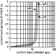
 Figure 3. Output Saturation Voltage vs Output Sink Current
 Figure 2. Input Bias Current vs Supply Current
 Figure 4. Input Offset Voltage vs Supply Voltage
7 Detailed Description
7.1 Overview
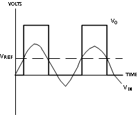
A comparator is often used to convert an analog signal to a digital signal. The comparator compares an input voltage (VIN) at the noninverting pin to the reference voltage (VREF) at the inverting pin. If VIN is less than VREF the output (VO) is low (VOL). However, if VIN is greater than VREF, the output voltage (VO) is high (VOH). Refer to Figure 6.
 Figure 5. Basic Comparator
 Figure 6. Basic Comparator Output
7.2 Functional Block Diagram

7.3 Feature Description
7.3.1 Input Stage
The LM397 has a bipolar input stage. The input common-mode voltage range is from 0 to (VS – 1.5 V).
7.3.2 Output Stage
The LM397 has an open-collector grounded-emitter NPN output transistor for the output stage. This requires an external pullup resistor connected between the positive supply voltage and the output. The external pullup resistor should be high enough resistance so to avoid excessive power dissipation. In addition, the pullup resistor should be low enough resistance to enable the comparator to switch with the load circuitry connected. Because it is an open-collector output stage, several comparator outputs can be connected together to create an OR’ing function output. With an open collector, the output can be used as a simple SPST switch to ground. The amount of current which the output can sink is approximately 10 mA. When the maximum current limit is reached, the output transistor will saturate and the output will rise rapidly (Figure 7).
7.4 Device Functional Modes
7.4.1 Hysteresis
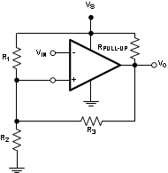
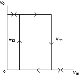
The basic comparator configuration may oscillate or produce a noisy output if the applied differential input is near the input offset voltage of the comparator. This tends to occur when the voltage on the input is equal or very close to the other input voltage. Adding hysteresis can prevent this problem. Hysteresis creates two switching thresholds (one for the rising input voltage and the other for the falling input voltage). Hysteresis is the voltage difference between the two switching thresholds. When both inputs are nearly equal, hysteresis causes one input to effectively move quickly pass the other. Thus, effectively moving the input out of region that oscillation may occur.
For an inverting configured comparator, hysteresis can be added with a three resistor network and positive feedback. When input voltage (VIN) at the inverting node is less than non-inverting node (VT), the output is high. The equivalent circuit for the three resistor network is R1 in parallel with R3 and in series with R2. The lower threshold voltage VT1 is calculated by Equation 1:
When VIN is greater than VT, the output voltage is low. The equivalent circuit for the three resistor network is R2 in parallel with R3 and in series with R1. The upper threshold voltage VT2 is calculated by Equation 2:
The hysteresis is defined in Equation 3:
 Figure 8. Inverting Configured Comparator - LM397

