SNAS491B February   2010  – February 2018 LM48580

PRODUCTION DATA.  

  1. Features
  2. Applications
  3. Description
    1.     Device Images
      1.      Typical Application
  4. Revision History
  5. Pin Configuration and Functions
    1.     Pin Functions
  6. Specifications
    1. 6.1 Absolute Maximum Ratings
    2. 6.2 ESD Ratings
    3. 6.3 Recommended Operating Conditions
    4. 6.4 Thermal Information
    5. 6.5 Electrical Characteristics: VDD = 3.6 V
    6. 6.6 Typical Performance Characteristics
  7. Parameter Measurement Information
  8. Detailed Description
    1. 8.1 Overview
    2. 8.2 Functional Block Diagram
    3. 8.3 Feature Description
      1. 8.3.1 Class H Operation
      2. 8.3.2 Properties of Piezoelectric Elements
      3. 8.3.3 Differential Amplifier Explanation
      4. 8.3.4 Thermal Shutdown
      5. 8.3.5 Gain Setting
    4. 8.4 Device Functional Modes
      1. 8.4.1 Shutdown Function
  9. Application and Implementation
    1. 9.1 Application Information
    2. 9.2 Typical Application
      1. 9.2.1 Design Requirements
        1. 9.2.1.1 Proper Selection of External Components
          1. 9.2.1.1.1 Boost Converter Capacitor Selection
      2. 9.2.2 Detailed Design Procedure
        1. 9.2.2.1 Boost Converter Output Capacitor Selection
          1. 9.2.2.1.1 Inductor Selection
          2. 9.2.2.1.2 Diode Selection
        2. 9.2.2.2 Application Curves
  10. 10Power Supply Recommendations
  11. 11Layout
    1. 11.1 Layout Guidelines
    2. 11.2 Layout Example
  12. 12Device and Documentation Support
    1. 12.1 Device Support
      1. 12.1.1 Development Support
        1. 12.1.1.1 Third-Party Products Disclaimer
    2. 12.2 Receiving Notification of Documentation Updates
    3. 12.3 Community Resources
    4. 12.4 Trademarks
    5. 12.5 Electrostatic Discharge Caution
    6. 12.6 Glossary
  13. 13Mechanical, Packaging, and Orderable Information

Package Options

Mechanical Data (Package|Pins)
Thermal pad, mechanical data (Package|Pins)
Orderable Information

Pin Configuration and Functions

DSBGA Package
YZR 12-Pin
Top View
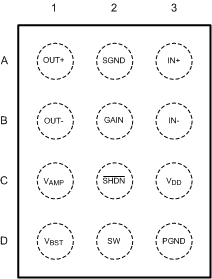
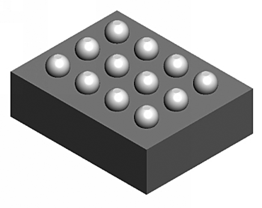
LM48580 30108071.gif
YZR0012 Package
(Bumps Up) View
LM48580 30108031.png

Pin Functions

BumpNameDescription
A1 OUT+ Amplifier Non-Inverting Output
A2 SGND Amplifier Ground
A3 IN+ Amplifier Non-Inverting Input
B1 OUT- Amplifier Inverting Output
B2 GAIN Gain Select:
GAIN = float: AV = 18dB
GAIN = GND: AV = 24dB
GAIN = VDD: AV = 30dB
B3 IN- Amplifier Inverting Input
C1 VAMP Amplifier Supply Voltage. Connect to VBST
C2 SHDN Active Low Shutdown. Drive SHDN low to disable device.
Connect SHDN to VDD for normal operation.
C3 VDD Power Supply
D1 VBST Boost Converter Output
D2 SW Boost Converter Switching Node
D3 PGND Boost Converter Ground