SNVSA90 December 2014 LM5021-Q1
PRODUCTION DATA.
- 1 Features
- 2 Applications
- 3 Description
- 4 Revision History
- 5 Pin Configuration and Functions
- 6 Specifications
- 7 Detailed Description
- 8 Application and Implementation
- 9 Power Supply Recommendations
- 10Layout
- 11Device and Documentation Support
- 12Mechanical, Packaging, and Orderable Information
Package Options
Mechanical Data (Package|Pins)
- DGK|8
Thermal pad, mechanical data (Package|Pins)
Orderable Information
10 Layout
10.1 Layout Guidelines
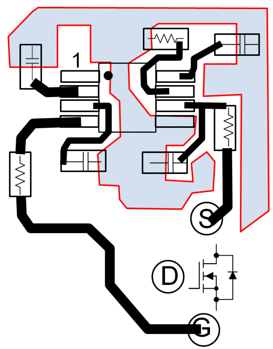
In addition to following general power management IC layout guidelines (star grounding, minimal current loops, reasonable impedance levels, and so on) layout for the LM5021 should take into account the following:
- If possible, a ground plane should be used to minimize the voltage drop on the ground circuit and the noise introduced by parasitic inductances in individual traces.
- A decoupling capacitor is required for both the VIN pin and VCC pin and both should be returned to GND as close to the IC as possible. VIN is the more critical capacitor and should take first priority when connecting to GND as close as possible to the IC.
- The timing setting components such as the RT pin resistor, SS pin capacitor should be directly connected to the ground plane or returned directly to the GND pin on their own traces.
- The CS pin filter capacitor should be as close to the IC possible and grounded right at the IC ground pin. This ensures the best filtering effect and minimizes the chance of current sense pin malfunction.
- Gate driver loop area should be minimized to reduce the EMI noise because of the high di/dt current in the loop.
10.2 Layout Example
 Figure 26. Layout Example
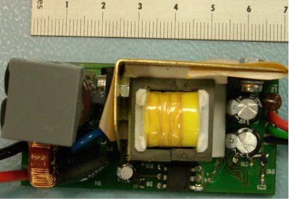
 Figure 27. Top Side View
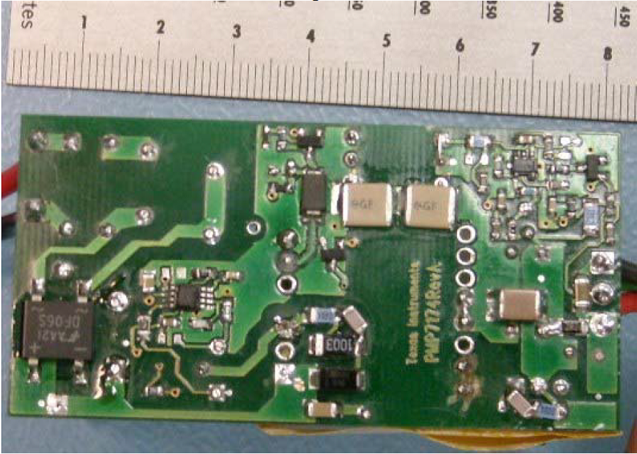
 Figure 28. Bottom Side View