-
LM5067 Negative Hot Swap / Inrush Current Controller with Power Limiting
- 1 Features
- 2 Applications
- 3 Description
- 4 Revision History
- 5 Device Comparison
- 6 Pin Configuration and Functions
- 7 Specifications
- 8 Detailed Description
-
9 Application and Implementation
- 9.1 Application Information
- 9.2
Typical Application
- 9.2.1 Design Requirements
- 9.2.2 Detailed Design Procedure
- 9.2.3 Application Curves
- 10Power Supply Recommendations
- 11Layout
- 12Device and Documentation Support
- 13Mechanical, Packaging, and Orderable Information
- IMPORTANT NOTICE
Package Options
Mechanical Data (Package|Pins)
Thermal pad, mechanical data (Package|Pins)
Orderable Information
LM5067 Negative Hot Swap / Inrush Current Controller with Power Limiting
1 Features
- Wide operating range: –9 V to –80 V
- In-rush current limit for safe board insertion into live power sources
- Programmable maximum power dissipation in the external pass device
- Adjustable current limit
- Circuit breaker function for severe overcurrent events
- Adjustable undervoltage lockout (UVLO) and hysteresis
- Adjustable overvoltage lockout (OVLO) and hysteresis
- Initial insertion timer allows ringing and transients to subside after system connection
- Programmable fault timer avoids nuisance trips
- Active high open drain POWER GOOD output
- Available in latched fault and automatic restart versions
2 Applications
- Server backplane systems
- In-Rush current limiting
- Solid state circuit breaker
- Transient voltage protector
- Solid state relay
- Undervoltage lock-out
- Power good detector and indicator
3 Description
The LM5067 negative hot swap controller provides intelligent control of the power supply connections during insertion and removal of circuit cards from a live system backplane or other “hot” power sources. The LM5067 provides in-rush current control to limit system voltage droop and transients. The current limit and power dissipation in the external series pass N-Channel MOSFET are programmable, ensuring operation within the Safe Operating Area (SOA). In addition, the LM5067 provides circuit protection by monitoring for over-current and over-voltage conditions. The POWER GOOD output indicates when the output voltage is close to the input voltage. The input under-voltage and over-voltage lockout levels and hysteresis are programmable, as well as the fault detection time. The LM5067-1 latches off after a fault detection, while the LM5067-2 automatically attempts restarts at a fixed duty cycle. The LM5067 is available in a 10-pin VSSOP package and a 14-pin SOIC package.
| PART NUMBER | PACKAGE | BODY SIZE (NOM) |
|---|---|---|
| LM5067 | VSSOP (10) | 3.00 mm x 3.00 mm |
| SOIC (14) | 8.99 mm x 7.49 mm |
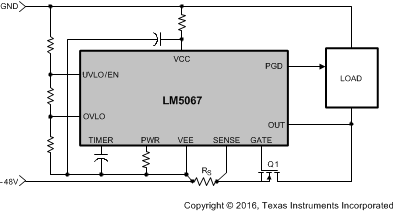
 Negative Power Bus In-Rush and Fault Protection
4 Revision History
Changes from Revision C (March 2013) to Revision D (August 2020)
- Added ESD Rating table, Feature Description section, Device Functional Modes, Application and Implementation section, Power Supply Recommendations section, Layout section, Device and Documentation Support section, and Mechanical, Packaging, and Orderable Information section Go
- Updated the numbering format for tables, figures and cross-references throughout the documentGo
- Updated Applications sectionGo
- Deleted text : "LM5067A is available..." Go
Changes from Revision B (September 2009) to Revision C (March 2013)
- Changed layout of National Data Sheet to TI formatGo
5 Device Comparison
| DEVICE NUMBER |
RETRY BEHAVIOR AFTER FAULT |
PACKAGE |
|---|---|---|
|
LM5067-1 |
Latch-off |
VSSOP (10), SOIC (14) |
| LM5067-2 |
Auto-retry |
VSSOP (10), SOIC (14) |
6 Pin Configuration and Functions
 Figure 6-1 10-Lead
VSSOPTop View
 Figure 6-2 14-Lead
SOICTop View