SNVSBV0A June 2021 – June 2021 LM5146
PRODUCTION DATA
- 1 Features
- 2 Applications
- 3 Description
- 4 Revision History
- 5 Description (continued)
- 6 Pin Configuration and Functions
- 7 Specifications
-
8 Detailed Description
- 8.1 Overview
- 8.2 Functional Block Diagram
- 8.3
Feature Description
- 8.3.1 Input Range (VIN)
- 8.3.2 Output Voltage Setpoint and Accuracy (FB)
- 8.3.3 High-Voltage Bias Supply Regulator (VCC)
- 8.3.4 Precision Enable (EN/UVLO)
- 8.3.5 Power Good Monitor (PGOOD)
- 8.3.6 Switching Frequency (RT, SYNCIN)
- 8.3.7 Configurable Soft Start (SS/TRK)
- 8.3.8 Voltage-Mode Control (COMP)
- 8.3.9 Gate Drivers (LO, HO)
- 8.3.10 Current Sensing and Overcurrent Protection (ILIM)
- 8.3.11 OCP Duty Cycle Limiter
- 8.4 Device Functional Modes
- 9 Application and Implementation
- 10Power Supply Recommendations
- 11Layout
- 12Device and Documentation Support
- 13Mechanical, Packaging, and Orderable Information
Package Options
Mechanical Data (Package|Pins)
- RGY|20
Thermal pad, mechanical data (Package|Pins)
- RGY|20
Orderable Information
8.3.3 High-Voltage Bias Supply Regulator (VCC)
The LM5146 contains an internal high-voltage VCC regulator that provides a bias supply for the PWM controller and its gate drivers for the external MOSFETs. The input pin (VIN) can be connected directly to an input voltage source up to 100 V. The output of the VCC regulator is set to 7.5 V. However, when the input voltage is below the VCC setpoint level, the VCC output tracks VIN with a small voltage drop. Connect a ceramic decoupling capacitor between 1 µF and 5 µF from VCC to AGND for stability.
The VCC regulator output has a current limit of 40 mA (minimum). At power up, the regulator sources current into the capacitor connected to the VCC pin. When the VCC voltage exceeds its rising UVLO threshold of 4.93 V, the output is enabled (if EN/UVLO is above 1.2 V), and the soft-start sequence begins. The output remains active until the VCC voltage falls below its falling UVLO threshold of 4.67 V (typical) or if EN/UVLO goes to a standby or shutdown state.
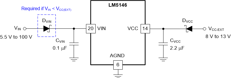
Internal power dissipation of the VCC regulator can be minimized by connecting the output voltage or an auxiliary bias supply rail (up to 13 V) to VCC using a diode DVCC as shown in Figure 8-2. A diode in series with the input prevents reverse current flow from VCC to VIN if the input voltage falls below the external VCC rail.
 Figure 8-2 VCC Bias Supply Connection From VOUT or Auxiliary Supply
Note that a finite bias supply regulator dropout voltage exists and is manifested to a larger extent when driving high gate charge (QG) power MOSFETs at elevated switching frequencies. For example, at VVIN = 6 V, the VCC voltage is 5.8 V with a DC operating current, IVCC, of 20 mA. Such a low gate drive voltage can be insufficient to fully enhance the power MOSFETs. At the very least, MOSFET on-state resistance, RDS(ON), can increase at such low gate drive voltage.
Here are the main considerations when operating at input voltages below 7.5 V:
- Increased MOSFET RDS(on) at lower VGS, leading to Increased conduction losses and reduced OCP setpoint
- Increased switching losses given the slower switching times when operating at lower gate voltages
- Restricted range of suitable power MOSFETs to choose from (MOSFETs with RDS(on) rated at VGS = 4.5 V become mandatory)