SNVSBI7B January 2020 – January 2021 LM5156-Q1 , LM51561-Q1
PRODUCTION DATA
- 1 Features
- 2 Applications
- 3 Description
- 4 Revision History
- 5 Description (continued)
- 6 Device Comparison Table
- 7 Pin Configuration and Functions
- 8 Specifications
-
9 Detailed Description
- 9.1 Overview
- 9.2 Functional Block Diagram
- 9.3
Feature Description
- 9.3.1 Line Undervoltage Lockout (UVLO/SYNC/EN Pin)
- 9.3.2 High Voltage VCC Regulator (BIAS, VCC Pin)
- 9.3.3 Soft Start (SS Pin)
- 9.3.4 Switching Frequency (RT Pin)
- 9.3.5 Dual Random Spread Spectrum (DRSS)
- 9.3.6 Clock Synchronization (UVLO/SYNC/EN Pin)
- 9.3.7 Current Sense and Slope Compensation (CS Pin)
- 9.3.8 Current Limit and Minimum On-time (CS Pin)
- 9.3.9 Feedback and Error Amplifier (FB, COMP Pin)
- 9.3.10 Power-Good Indicator (PGOOD pin)
- 9.3.11 Hiccup Mode Overload Protection (LM51561-Q1 Only)
- 9.3.12 Maximum Duty Cycle Limit and Minimum Input Supply Voltage
- 9.3.13 MOSFET Driver (GATE Pin)
- 9.3.14 Overvoltage Protection (OVP)
- 9.3.15 Thermal Shutdown (TSD)
- 9.4 Device Functional Modes
- 10Application and Implementation
- 11Power Supply Recommendations
- 12Layout
- 13Device and Documentation Support
- 14Mechanical, Packaging, and Orderable Information
Package Options
Mechanical Data (Package|Pins)
- DSS|12
Thermal pad, mechanical data (Package|Pins)
- DSS|12
Orderable Information
9.3.5 Dual Random Spread Spectrum (DRSS)
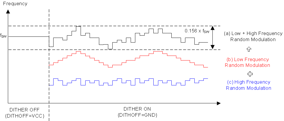
The device provides a digital spread spectrum which reduces the EMI of the power supply over a wide frequency range. This function is dynamically selectable during operation. The internal modulator dithers the internal clock when the DITHOFF pin is less than 1.0 V or the pin is grounded, and it stops clock dithering when the DITHOFF pin is greater than 2.0 V or the pin is connected to VCC. When an external synchronization clock is applied to the SYNC pin, the internal spread spectrum is disabled. DRSS (a) combines a low-frequency triangular modulation profile (b) with a high frequency cycle-by-cycle random modulation profile (c). The low frequency triangular modulation improves performance in lower radio frequency bands (for example, the AM band), while the high frequency random modulation improves performance in higher radio frequency bands (for example, the FM band). In addition, the frequency of the triangular modulation is further modulated randomly to reduce the likelihood of any audible tones. To minimize output voltage ripple caused by spread spectrum, duty cycle is modified on a cycle-by-cycle basis to maintain a nearly constant duty cycle when dithering is enabled (see Figure 9-10).
 Figure 9-10 Dual Random Spread
Spectrum