SNVSBK7A july 2021 – august 2023 LM5157
PRODUCTION DATA
- 1
- 1 Features
- 2 Applications
- 3 Description
- 4 Revision History
- 5 Device Comparison Table
- 6 Pin Configuration and Functions
- 7 Specifications
-
8 Detailed Description
- 8.1 Overview
- 8.2 Functional Block Diagram
- 8.3
Feature Description
- 8.3.1 Line Undervoltage Lockout (UVLO/SYNC/EN Pin)
- 8.3.2 High Voltage VCC Regulator (BIAS, VCC Pin)
- 8.3.3 Soft Start (SS Pin)
- 8.3.4 Switching Frequency (RT Pin)
- 8.3.5 Dual Random Spread Spectrum – DRSS (MODE Pin)
- 8.3.6 Clock Synchronization (UVLO/SYNC/EN Pin)
- 8.3.7 Current Sense and Slope Compensation
- 8.3.8 Current Limit and Minimum On Time
- 8.3.9 Feedback and Error Amplifier (FB, COMP Pin)
- 8.3.10 Power-Good Indicator (PGOOD Pin)
- 8.3.11 Hiccup Mode Overload Protection (MODE Pin)
- 8.3.12 Maximum Duty Cycle Limit and Minimum Input Supply Voltage
- 8.3.13 Internal MOSFET (SW Pin)
- 8.3.14 Overvoltage Protection (OVP)
- 8.3.15 Thermal Shutdown (TSD)
- 8.4 Device Functional Modes
- 9 Application and Implementation
- 10Power Supply Recommendations
- 11Layout
- 12Device and Documentation Support
- 13Mechanical, Packaging, and Orderable Information
Package Options
Mechanical Data (Package|Pins)
- RTE|16
Thermal pad, mechanical data (Package|Pins)
- RTE|16
Orderable Information
8.3.6 Clock Synchronization (UVLO/SYNC/EN Pin)
The switching frequency of the device can be synchronized to an external clock by pulling down the EN/UVLO/SYNC pin. The internal clock of the device is synchronized at the falling edge, but ignores the falling edge input during the forced off time, which is determined by the maximum duty cycle limit. The external synchronization clock must pull down the EN/UVLO/SYNC pin voltage below VUVLO(FALLING). The duty cycle of the pulldown pulse is not limited, but the minimum pulldown pulse width must be greater than 150 ns. The minimum pullup pulse width must be greater than 250 ns. Figure 8-10 shows an implementation of the remote shutdown function. The UVLO pin can be pulled down by a discrete MOSFET or an open-drain output of an MCU. In this configuration, the device stops switching immediately after the UVLO pin is grounded, and the device shuts down 40 µs (typical) after the UVLO pin is grounded.
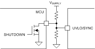 Figure 8-10 UVLO and Shutdown
Figure 8-11 shows an implementation of shutdown and clock synchronization functions together. In this configuration, the device immediately stops switching when the UVLO pin is grounded, and the device shuts down if the fSYNC stays in high logic state for longer than 40 µs (typical). UVLO is in low logic state for more than 40 µs (typical). The device runs at fSYNC if clock pulses are provided after the device is enabled.
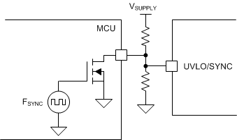 Figure 8-11 UVLO, Shutdown, and Clock Synchronization
Figure 8-13 and Figure 8-14 show implementations of standby and clock synchronization functions together. In this configuration, The device stops switching immediately if fSYNC stays in high logic state and enters Standby mode if fSYNC stays in high logic state for longer than two switching cycles. The device runs at fSYNC if clock pulses are provided. Since the device can be enabled when the UVLO pin voltage is greater than the enable threshold for more than 1.5 µs, the configurations in Figure 8-13 and Figure 8-14 are recommended if the external clock synchronization pulses are provided from the start before the device is enabled. This 1.5-µs requirement can be relaxed when the duty cycle of the synchronization pulse is greater than 50%. Figure 8-12 shows the required minimum duty cycle to start up by synchronization pulses. When the switching frequency is greater than 1.1 MHz, the UVLO pin voltage must be greater than the enable threshold for more than 1.5 µs before applying the external synchronization pulse.
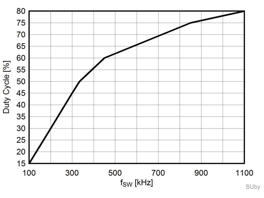 Figure 8-12 Required Duty Cycle to Start-Up by External Synchronization Clock
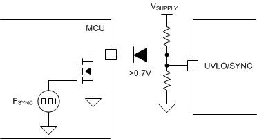 Figure 8-13 UVLO, Standby, and Clock Synchronization (a)
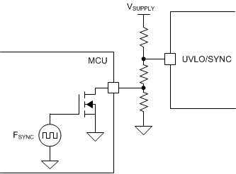 Figure 8-14 UVLO, Standby, and Clock Synchronization (b)
If the UVLO function is not required, the shutdown and clock synchronization functions can be implemented together by using one push-pull output of the MCU. In this configuration, the device shuts down if fSYNC stays in low logic state for longer than 40 µs (typical). The device is enabled if fSYNC stays in high logic state for longer than 1.5 µs. The device runs at fSYNC if clock pulses are provided after the device is enabled. Also, in this configuration, it is recommended to apply the external clock pulses after the BIAS is supplied. By limiting the current flowing into the UVLO pin below 1 mA using a current limiting resistor, the external clock pulses can be supplied before the BIAS is supplied (see Figure 8-15).
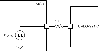 Figure 8-15 Shutdown and Clock Synchronization
Figure 8-16 shows an implementation of inverted enable using external circuit.
 Figure 8-16 Inverted UVLO
The external clock frequency (fSYNC) must be within +25% and –30% of fRT(TYPICAL). Since the maximum duty cycle limit and the peak current limit with a slope resistor (RSL) are affected by the clock synchronization, take extra care when using the clock synchronization function. See Section 8.3.7 and Section 8.3.12 for more information.