SNVSBS7B December   2021  – December 2024 LM5168 , LM5169

PRODUCTION DATA  

  1.   1
  2. Features
  3. Applications
  4. Description
  5. Device Comparison Table
  6. Pin Configuration and Functions
  7. Specifications
    1. 6.1 Absolute Maximum Ratings
    2. 6.2 ESD Ratings
    3. 6.3 Recommended Operating Conditions
    4. 6.4 Thermal Information
    5. 6.5 Electrical Characteristics
    6. 6.6 Typical Characteristics
  8. Detailed Description
    1. 7.1 Overview
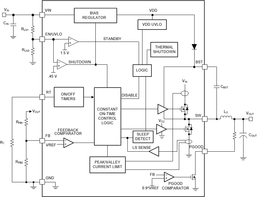
    2. 7.2 Functional Block Diagram
    3. 7.3 Feature Description
      1. 7.3.1  Control Architecture
      2. 7.3.2  Internal VCC Regulator and Bootstrap Capacitor
      3. 7.3.3  Internal Soft Start
      4. 7.3.4  On-Time Generator
      5. 7.3.5  Current Limit
      6. 7.3.6  N-Channel Buck Switch and Driver
      7. 7.3.7  Synchronous Rectifier
      8. 7.3.8  Enable, Undervoltage Lockout (EN/UVLO)
      9. 7.3.9  Power Good (PGOOD)
      10. 7.3.10 Thermal Protection
    4. 7.4 Device Functional Modes
      1. 7.4.1 Shutdown Mode
      2. 7.4.2 Active Mode
      3. 7.4.3 Sleep Mode
  9. Application and Implementation
    1. 8.1 Application Information
    2. 8.2 Typical Fly-Buck™ Converter Application
      1. 8.2.1 Design Requirements
      2. 8.2.2 Detailed Design Procedure
        1. 8.2.2.1  Switching Frequency (RT)
        2. 8.2.2.2  Transformer Selection
        3. 8.2.2.3  Output Capacitor Selection
        4. 8.2.2.4  Secondary Output Diode
        5. 8.2.2.5  Setting Output Voltage
        6. 8.2.2.6  Input Capacitor
        7. 8.2.2.7  Type-3 Ripple Network
        8. 8.2.2.8  CBST Selection
        9. 8.2.2.9  Minimum Secondary Output Load
        10. 8.2.2.10 Example Design Summary
      3. 8.2.3 Application Curves
    3. 8.3 Typical Buck Application
      1. 8.3.1 Design Requirements
      2. 8.3.2 Detailed Design Procedure
        1. 8.3.2.1 Switching Frequency (RT)
        2. 8.3.2.2 Buck Inductor Selection
        3. 8.3.2.3 Setting the Output Voltage
        4. 8.3.2.4 Type-3 Ripple Network
        5. 8.3.2.5 Output Capacitor Selection
        6. 8.3.2.6 Input Capacitor Considerations
        7. 8.3.2.7 CBST Selection
        8. 8.3.2.8 Example Design Summary
      3. 8.3.3 Application Curves
    4. 8.4 Power Supply Recommendations
    5. 8.5 Layout
      1. 8.5.1 Thermal Considerations
      2. 8.5.2 Typical EMI Results
      3. 8.5.3 Layout Guidelines
        1. 8.5.3.1 Compact PCB Layout for EMI Reduction
        2. 8.5.3.2 Feedback Resistors
      4. 8.5.4 Layout Example
  10. Device and Documentation Support
    1. 9.1 Device Support
      1. 9.1.1 Third-Party Products Disclaimer
    2. 9.2 Documentation Support
      1. 9.2.1 Related Documentation
    3. 9.3 Receiving Notification of Documentation Updates
    4. 9.4 Support Resources
    5. 9.5 Trademarks
    6. 9.6 Electrostatic Discharge Caution
    7. 9.7 Glossary
  11. 10Revision History
  12. 11Mechanical, Packaging, and Orderable Information

Package Options

Mechanical Data (Package|Pins)
Thermal pad, mechanical data (Package|Pins)
Orderable Information

Functional Block Diagram

LM5168 LM5169