SNVSBS7B December 2021 – December 2024 LM5168 , LM5169
PRODUCTION DATA
- 1
- 1 Features
- 2 Applications
- 3 Description
- 4 Device Comparison Table
- 5 Pin Configuration and Functions
- 6 Specifications
-
7 Detailed Description
- 7.1 Overview
- 7.2 Functional Block Diagram
- 7.3
Feature Description
- 7.3.1 Control Architecture
- 7.3.2 Internal VCC Regulator and Bootstrap Capacitor
- 7.3.3 Internal Soft Start
- 7.3.4 On-Time Generator
- 7.3.5 Current Limit
- 7.3.6 N-Channel Buck Switch and Driver
- 7.3.7 Synchronous Rectifier
- 7.3.8 Enable, Undervoltage Lockout (EN/UVLO)
- 7.3.9 Power Good (PGOOD)
- 7.3.10 Thermal Protection
- 7.4 Device Functional Modes
-
8 Application and Implementation
- 8.1 Application Information
- 8.2
Typical Fly-Buck™ Converter Application
- 8.2.1 Design Requirements
- 8.2.2
Detailed Design Procedure
- 8.2.2.1 Switching Frequency (RT)
- 8.2.2.2 Transformer Selection
- 8.2.2.3 Output Capacitor Selection
- 8.2.2.4 Secondary Output Diode
- 8.2.2.5 Setting Output Voltage
- 8.2.2.6 Input Capacitor
- 8.2.2.7 Type-3 Ripple Network
- 8.2.2.8 CBST Selection
- 8.2.2.9 Minimum Secondary Output Load
- 8.2.2.10 Example Design Summary
- 8.2.3 Application Curves
- 8.3 Typical Buck Application
- 8.4 Power Supply Recommendations
- 8.5 Layout
- 9 Device and Documentation Support
- 10Revision History
- 11Mechanical, Packaging, and Orderable Information
Package Options
Mechanical Data (Package|Pins)
Thermal pad, mechanical data (Package|Pins)
- DDA|8
Orderable Information
3 Description
The LM5169 and LM5168 synchronous buck converters are designed to regulate over a wide input voltage range, minimizing the need for external surge suppression components. A minimum controllable on time of 50ns facilitates large step-down conversion ratios, enabling the direct step-down from a 48V nominal input to low-voltage rails for reduced system complexity and design cost. The LM516x operates during input voltage dips as low as 6V, at nearly 100% duty cycle if needed, making the device an excellent choice for wide input supply range industrial and high cell count battery pack applications.
With integrated high-side and low-side power MOSFETs, the LM5169 delivers up to 0.65A of output current and the LM5168 delivers up to 0.3A of output current. A constant on-time (COT) control architecture provides nearly constant switching frequency with excellent load and line transient response. The LM516x is available in FPWM or auto mode versions. FPWM mode provides forced CCM operation across the entire load range supporting isolated Fly-Buck converter applications. Auto mode enables ultra-low IQ and diode emulation mode operation for high light-load efficiency.
| PART NUMBER(3) | PACKAGE(1) | PACKAGE SIZE(2) |
|---|---|---|
| LM5169 | DDA (HSOIC, 8) | 4.9mm × 6mm |
| NGU (WSON, 8) | 4.00mm × 4.00mm | |
| LM5168 | DDA (HSOIC, 8) | 4.9mm × 6mm |
| NGU (WSON, 8) | 4.00mm × 4.00mm |
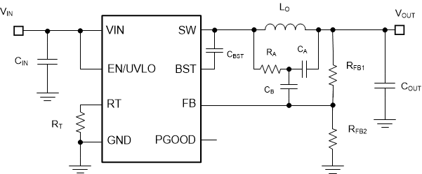
 Typical Buck Application Circuit
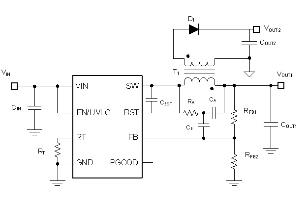
 Typical Fly-Buck™ Converter
Application Circuit