SNVSBU4F June 2022 – January 2025 LM5177
PRODUCTION DATA
- 1
- 1 Features
- 2 Applications
- 3 Description
- 4 Pin Configuration and Functions
- 5 Specifications
- 6 Parameter Measurement Information
-
7 Detailed Description
- 7.1 Overview
- 7.2 Functional Block Diagram
- 7.3
Feature Description
- 7.3.1 Power-On Reset (POR System)
- 7.3.2 Buck-Boost Control Scheme
- 7.3.3 Power Save Mode
- 7.3.4 Supply Voltage Selection – VMAX Switch
- 7.3.5 Enable and Undervoltage Lockout
- 7.3.6 Oscillator Frequency Selection
- 7.3.7 Frequency Synchronization
- 7.3.8 Voltage Regulation Loop
- 7.3.9 Output Voltage Tracking
- 7.3.10 Slope Compensation
- 7.3.11 Configurable Soft Start
- 7.3.12 Peak Current Sensor
- 7.3.13 Current Monitoring and Current Limit Control Loop
- 7.3.14 Short Circuit - Hiccup Protection
- 7.3.15 nFLT Pin and Protections
- 7.3.16 Device Configuration Pin
- 7.3.17 Dual Random Spread Spectrum – DRSS
- 7.3.18 Gate Driver
- 7.4 Device Functional Modes
-
8 Application and Implementation
- 8.1 Application Information
- 8.2
Typical Application
- 8.2.1 Design Requirements
- 8.2.2
Detailed Design Procedure
- 8.2.2.1 Custom Design with WEBENCH Tools
- 8.2.2.2 Frequency
- 8.2.2.3 Feedback Divider
- 8.2.2.4 Inductor and Current Sense Resistor Selection
- 8.2.2.5 Slope Compensation
- 8.2.2.6 Output Capacitor
- 8.2.2.7 Input Capacitor
- 8.2.2.8 UVLO Divider
- 8.2.2.9 Soft-Start Capacitor
- 8.2.2.10 MOSFETs QH1 and QL1
- 8.2.2.11 MOSFETs QH2 and QL2
- 8.2.2.12 Frequency Compensation
- 8.2.2.13 External Component Selection
- 8.2.3 Application Curves
- 9 Power Supply Recommendations
- 10Layout
- 11Device and Documentation Support
- 12Revision History
- 13Mechanical, Packaging, and Orderable Information
Package Options
Mechanical Data (Package|Pins)
- DCP|38
Thermal pad, mechanical data (Package|Pins)
- DCP|38
Orderable Information
7.4 Device Functional Modes
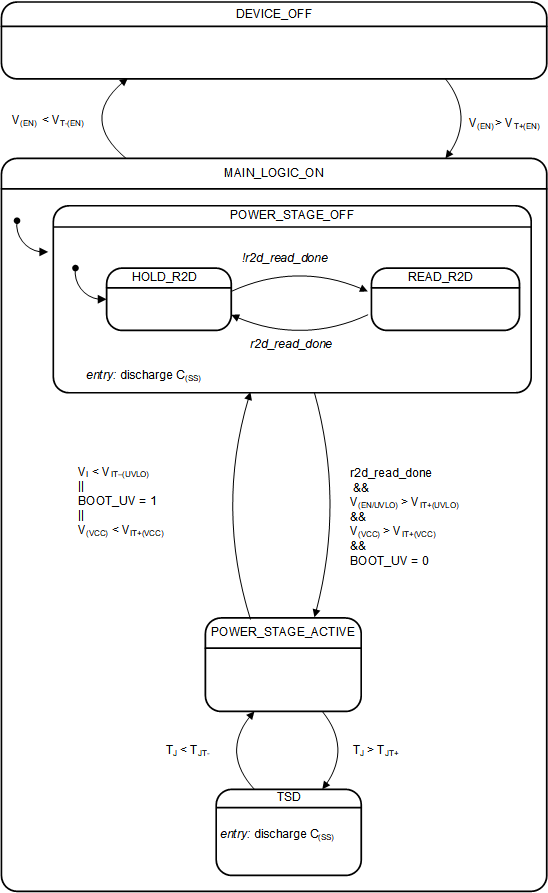
Figure 7-21 describes the functional behavior of the internal device logic.

Figure 7-21 Functional State Diagram
DEVICE_OFF
During the DEVICE_OFF state the LM5177 is in shutdown. All internal logic and the DC/DC converter as well as the gate driver are off. The internal POR- system monitors the EN threshold to start the initialization of the reference system an device logic. The device current consumption is given by the shutdown current.
MAIN_LOGIC_ON
Once the LM5177 transits to the MAIN_LOGIC_ON state it will first stay in the POWER_STAGE_OFF state. Here the necessary checks and preparation for the start up are taken. The current consumption is given by the standby current.
HOLD-R2D
In this state the CFG-pin settings are read and the logic is storing this settings until the next EN -pin cycle.
READ_R2D
During the READ-R2D state the LM5177 executives the reading of the CFG-pin to get the selected settings determined by placed resistor.
POWER_STAGE_ACTIVE
The device executes the soft-start ramp during each entry to this state to avoid excessive inrush currents. In this state the power stage is active and the converter in operation. The current consumption is given by the active quiescent current of the electrical specification table.
TSD
The device enters the TSD-state if the silicon junction temperature exceeds the thermal shutdown limit. It automatically transits back to the POWER_STAGE_ACTIVE -state once the hysteresis of the thermal shutdown triggers.